This thread has been locked.

If you have a related question, please click the "Ask a related question" button in the top right corner. The newly created question will be automatically linked to this question.

[参考译文] TM4C1294NCPDT:ADC 模拟信号:AIN16-19 (IO PK1-3)在软件中不工作

Guru**** 2609215 points


请注意,本文内容源自机器翻译,可能存在语法或其它翻译错误,仅供参考。如需获取准确内容,请参阅链接中的英语原文或自行翻译。

https://e2e.ti.com/support/microcontrollers/arm-based-microcontrollers-group/arm-based-microcontrollers/f/arm-based-microcontrollers-forum/1427682/tm4c1294ncpdt-adc-analog-signals-ain16-19-io-pk1-3-not-working-in-software

器件型号:TM4C1294NCPDT

工具与软件:

您好!

我按如下方式配置 ADC 模拟输入:

ROM_GPIOPinTypeADC (GPIO_PORTK_BASE、GPIO_PIN_0);  // AIN16

ROM_GPIOPinTypeADC (GPIO_PORTK_BASE、GPIO_PIN_1);  // AIN17

ROM_GPIOPinTypeADC (GPIO_PORTK_BASE、GPIO_PIN_2);  // AIN18

ROM_GPIOPinTypeADC (GPIO_PORTK_BASE、GPIO_PIN_3);  // AIN19

然后尝试从其中读取值:

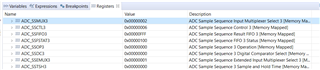
ADCSequenceConfigure (ADC0_BASE、3、ADC_TRIGGER_processor、0);

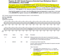
ADCSequenceStepConfigure (ADC0_BASE、3、0、ADC_CTL_CH16 | ADC_CTL_IE |)
ADC_CTL_END);                                                             //以此类推  


//
//由于现在配置了采样序列3、因此必须启用它。
//
ADCSequenceEnable (ADC0_BASE、3);

//
//清除中断状态标志。 这样做是为了确保
//在我们采样之前清除中断标志。
//
ADCIntClear (ADC0_BASE、3);

//
//对温度传感器进行永久采样。 在上显示该值
//控制台。
//
while (1)

//
//触发 ADC 转换。
//
ADCProcessorTrigger (ADC0_BASE、3);

//
//等待转换完成。
//
while (! ADCIntStatus (ADC0_BASE、3、false)

}

//
//清除 ADC 中断标志。
//
ADCIntClear (ADC0_BASE、3);

//
//读取 ADC 值。
//
ADCSequenceDataGet (ADC0_BASE、3、ADCValues);

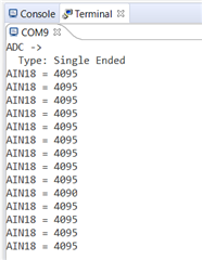
其他 AIN0-15运行正常、我可以读取它们的值。

与我一起工作的硬件工程师能够触碰引脚(相应地触碰18-21)并查看所需值。  

任何帮助都将受到 赞赏,

Tzipi

  • 请注意,本文内容源自机器翻译,可能存在语法或其它翻译错误,仅供参考。如需获取准确内容,请参阅链接中的英语原文或自行翻译。

    您好!

     您能否详细说明哪些不适用于 AIN16-AIN19? 是读取随机值还是实际发生了什么? 您是否可以读取 ADCSSEMUX3和 ADCSSMUX3 寄存器? 我只想知道您是否在 AIN[19:16]中复用。  

  • 请注意,本文内容源自机器翻译,可能存在语法或其它翻译错误,仅供参考。如需获取准确内容,请参阅链接中的英语原文或自行翻译。

    尊敬的 Charles:

    感谢您的答复。

    我正在从 AIN16-19读取随机值。

    我  在调试代码时读取寄存器 ADCSSEMUX3和 ADCSSMUX3、这两个寄存器的值均为0。

    好的、我知道  在开始 读取 AIN16-19之前、需要将 ADCSSEMUX3寄存器设置为1。  

    我不知道如何设置、您能帮忙吗? 我应该使用哪个函数来执行此操作?

    在读取 AIN16-19值之前、我还需要做什么其他事情吗?

    谢谢!

    Tzipi

  • 请注意,本文内容源自机器翻译,可能存在语法或其它翻译错误,仅供参考。如需获取准确内容,请参阅链接中的英语原文或自行翻译。

    您好!

     您是否可以尝试 使用 HWREG()函数手动写入 ADCSSEMUX3? 我目前在旅行。 如果需要、我今天稍后会展示一个使用 HWREG 的示例。  

  • 请注意,本文内容源自机器翻译,可能存在语法或其它翻译错误,仅供参考。如需获取准确内容,请参阅链接中的英语原文或自行翻译。

    我会在这里试用并更新您的信息、谢谢!

  • 请注意,本文内容源自机器翻译,可能存在语法或其它翻译错误,仅供参考。如需获取准确内容,请参阅链接中的英语原文或自行翻译。

    尊敬的 Charles:

    我成功地  用 HWREG()函数写入 ADCSSEMUX3。  

    如果我在 上面的所有代码之前这么做-它不会改变 AIN16-19的读取值-就像之前那样:读取一些随机值和 AIN17-19得到相同的值、而它们应该不同... (在执行 HWREG()函数之前也是如此)。

    如果我在 ADCSequenceDataGet 函数读取零之前执行此操作、

    我注意到您从数据表发给我的页面中的注释:  

    这意味着什么?

    寄存器 ADCSSCTL3的值在运行期间为0x00000007。

  • 请注意,本文内容源自机器翻译,可能存在语法或其它翻译错误,仅供参考。如需获取准确内容,请参阅链接中的英语原文或自行翻译。

    尊敬的 Tzipi:

     很抱歉我刚从旅行回来。 我在 LaunchPad 上将 PK2连接到3.3V 的情况下为 AIN18运行以下代码。 我可以看到它转换为4096。 请在下面找到这些信息、您能试一下吗?

    #include <stdbool.h>
    #include <stdint.h>
    #include "inc/hw_memmap.h"
    #include "driverlib/adc.h"
    #include "driverlib/gpio.h"
    #include "driverlib/pin_map.h"
    #include "driverlib/sysctl.h"
    #include "driverlib/uart.h"
    #include "utils/uartstdio.h"
    
    //*****************************************************************************
    //
    //! \addtogroup adc_examples_list
    //! <h1>Single Ended ADC (single_ended)</h1>
    //!
    //! This example shows how to setup ADC0 as a single ended input and take a
    //! single sample on AIN18/PK2.
    //!
    //! This example uses the following peripherals and I/O signals.  You must
    //! review these and change as needed for your own board:
    //! - ADC0 peripheral
    //! - GPIO Port E peripheral (for AIN18 pin)
    //! - AIN18 - PK2
    //!
    //! The following UART signals are configured only for displaying console
    //! messages for this example.  These are not required for operation of the
    //! ADC.
    //! - UART0 peripheral
    //! - GPIO Port A peripheral (for UART0 pins)
    //! - UART0RX - PA0
    //! - UART0TX - PA1
    //!
    //! This example uses the following interrupt handlers.  To use this example
    //! in your own application you must add these interrupt handlers to your
    //! vector table.
    //! - None.
    //
    //*****************************************************************************
    #define USER_LED1  GPIO_PIN_2
    
    #define SEQNUM 3
    //*****************************************************************************
    //
    // This function sets up UART0 to be used for a console to display information
    // as the example is running.
    //
    //*****************************************************************************
    void
    InitConsole(void)
    {
        //
        // Enable GPIO port A which is used for UART0 pins.
        // TODO: change this to whichever GPIO port you are using.
        //
        SysCtlPeripheralEnable(SYSCTL_PERIPH_GPIOA);
    
        //
        // Configure the pin muxing for UART0 functions on port A0 and A1.
        // This step is not necessary if your part does not support pin muxing.
        // TODO: change this to select the port/pin you are using.
        //
        GPIOPinConfigure(GPIO_PA0_U0RX);
        GPIOPinConfigure(GPIO_PA1_U0TX);
    
        //
        // Enable UART0 so that we can configure the clock.
        //
        SysCtlPeripheralEnable(SYSCTL_PERIPH_UART0);
    
        //
        // Use the internal 16MHz oscillator as the UART clock source.
        //
        UARTClockSourceSet(UART0_BASE, UART_CLOCK_SYSTEM);
    
        //
        // Select the alternate (UART) function for these pins.
        // TODO: change this to select the port/pin you are using.
        //
        GPIOPinTypeUART(GPIO_PORTA_BASE, GPIO_PIN_0 | GPIO_PIN_1);
    
        //
        // Initialize the UART for console I/O.
        //
        UARTStdioConfig(0, 115200, 120000000);
    }
    
    //*****************************************************************************
    //
    // Configure ADC0 for a single-ended input and a single sample.  Once the
    // sample is ready, an interrupt flag will be set.  Using a polling method,
    // the data will be read then displayed on the console via UART0.
    //
    //*****************************************************************************
    int
    main(void)
    {
        uint32_t ui32SysClock;
    
        //
        // This array is used for storing the data read from the ADC FIFO.
        //
        uint32_t pui32ADC0Value[0];
    
        //
        // Set the clocking to run at 20 MHz (200 MHz / 10) using the PLL.  When
        // using the ADC, you must either use the PLL or supply a 16 MHz clock
        // source.
        // TODO: The SYSCTL_XTAL_ value must be changed to match the value of the
        // crystal on your board.
        //
    
        ui32SysClock = SysCtlClockFreqSet((SYSCTL_XTAL_25MHZ |
                                           SYSCTL_OSC_MAIN |
                                           SYSCTL_USE_PLL |
                                           SYSCTL_CFG_VCO_240), 120000000);
    
        //
        // Set up the serial console to use for displaying messages.  This is
        // just for this example program and is not needed for ADC operation.
        //
        InitConsole();
    
        //
        // Display the setup on the console.
        //
        UARTprintf("ADC ->\n");
        UARTprintf("  Type: Single Ended\n");
    
        //
        // The ADC0 peripheral must be enabled for use.
        //
        SysCtlPeripheralEnable(SYSCTL_PERIPH_ADC0);
    
        SysCtlPeripheralEnable(SYSCTL_PERIPH_GPIOK);
    
        /*
         * ADC Clock runs at 30Mhz
         */
    //    ADCClockConfigSet(ADC0_BASE, ADC_CLOCK_SRC_PLL, 10);
    
    
        /* PK2 - AIN18
         */
    
        GPIOPinTypeADC(GPIO_PORTK_BASE, GPIO_PIN_2 );
    
        ADCSequenceConfigure(ADC0_BASE, SEQNUM, ADC_TRIGGER_PROCESSOR, 0);
    
        ADCSequenceStepConfigure(ADC0_BASE, SEQNUM, 0, ADC_CTL_CH18 | ADC_CTL_IE |
                                 ADC_CTL_END);
    
        ADCSequenceEnable(ADC0_BASE, SEQNUM);
    
        ADCIntClear(ADC0_BASE, SEQNUM);
    
        while(1)
        {
    
    
            //
            // Trigger the ADC conversion.
            //
    
            ADCProcessorTrigger(ADC0_BASE, SEQNUM);
    
            //
            // Wait for conversion to be completed.
            //
            while(!ADCIntStatus(ADC0_BASE, SEQNUM, false))
            {
            }
    
            //
            // Clear the ADC interrupt flag.
            //
            ADCIntClear(ADC0_BASE, SEQNUM);
    
            //
            // Read ADC Value.
            //
            ADCSequenceDataGet(ADC0_BASE, SEQNUM, pui32ADC0Value);
    
            //
            // Display the AIN18 (PK2) digital value on the console.
            //
            UARTprintf("AIN18 = %4d\n", pui32ADC0Value[0]);
    
            //
            // This function provides a means of generating a constant length
            // delay.  The function delay (in cycles) = 3 * parameter.  Delay
            // 250ms arbitrarily.
            //
    
            SysCtlDelay(ui32SysClock / 100);
    
        }
    }
    

    对于上面的代码我使用、采样序列3被使用。 以下是与 SS3相关的寄存器设置。  

  • 请注意,本文内容源自机器翻译,可能存在语法或其它翻译错误,仅供参考。如需获取准确内容,请参阅链接中的英语原文或自行翻译。

    我发现了我的错误! 谢谢你!!