Other Parts Discussed in Thread: TLV320ADC5140, PCM5122
请注意,本文内容源自机器翻译,可能存在语法或其它翻译错误,仅供参考。如需获取准确内容,请参阅链接中的英语原文或自行翻译。
器件型号:TLV320ADC5140 主题中讨论的其他器件: PCM5122
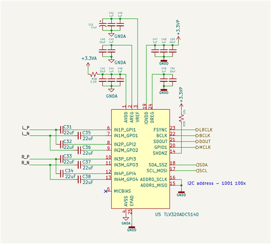
我们尝试在 I2S 主控模式下测试 TLV320ADC5140、根据我们的理解、为 MCLK 供电是可选的。 由于我们仅以48kHz 相关的采样率运行、因此 OUT PCB 具有用于单个24.576mhz 晶体的焊盘。 目前、XO 未组装。 我们的理解是、TLV320可以提供其自身的内部 BCK 和 LRCK 输出、但根据以下序列、我们不会得到 I2S BCK/LRCK。 原理图如下:
我们尝试使用此序列进行激活(伪代码、使用 node.js 和 i2c 库、将按照下面的确认写入寄存器):
    const MST_CFG1_RATES = {
        48 : 0x48, // 01001000
        96 : 0x58, // 01011000
        192: 0x68, // 01101000
        384: 0x78 // 01111000
    };

    // SLEEP_CFG wake
    await i2cWriteByte(0x02, 0x91);

    // MST_CFG0 master, 48k 10000111
    await i2cWriteByte(0x13, 0x87);

    // i2cWriteByte(0x16, 0xXX); // CLK_SRC master (not using for now)

    // 256x 96k, 01011000
    await i2cWriteByte(0x14, MST_CFG1_RATES[96]);

    // ASI_CFG0 i2s, 32bit, 01110000 ? (not sure about last two bits)
    await i2cWriteByte(0x07, 0x70);

    // DSP_CFG sum pairs 00000100 ? not sure about HP
    await i2cWriteByte(0x6B, 0x04);

    // DEV_STS0 power up 1-4? 11110000
    await i2cWriteByte(0x76, 0xF0);

    // IN_CH_EN enable input 1-4? 11110000
    await i2cWriteByte(0x73, 0xF0);

    // ASI_OUT_CH_EN enable 1,2? 11000000
    await i2cWriteByte(0x74, 0xC0);

    // CH1_CFG0 config input, line, single-ended, no dre, 20k: 10101000
    await i2cWriteByte(0x3C, 0xA8);

    // CH2_CFG0
    await i2cWriteByte(0x41, 0xA8);

    // CH3_CFG0
    await i2cWriteByte(0x46, 0xA8);

    // CH4_CFG0
    await i2cWriteByte(0x4B, 0xA8);
读取 i2c 并得到确认值:
{
  '0x02': '10010001',
  '0x13': '10000111',
  '0x14': '1011000',
  '0x07': '1110000',
  '0x6B': '100',
  '0x76': '0',
  '0x73': '11110000'
}
0x76看起来没有设置。 我们仍然希望在 FSYNC 和 BCLK 上看到生命体征。 GPIO1上是否需要 XO 输入? 数据表使其看起来是可选的、因此我们希望在没有数据表的情况下测试性能。 此外、该 I2S 主器件是同一电路板上 PCM5122的主器件。 但还没有这么远。