请注意,本文内容源自机器翻译,可能存在语法或其它翻译错误,仅供参考。如需获取准确内容,请参阅链接中的英语原文或自行翻译。
器件型号:TLV320AIC3101 您好!
我正在此处跟进之前的 TT:
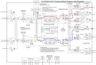
我们将使用上述硬件和突出显示的音频路径。 我们使编解码器可用、并且仅在左侧通道上发出音调。 但是、可以在左右两个耳机上听到音频音。 我已经查看了所有寄存器设置、但看不到任何明显的情况。 我可以将其中一个 DAC 静音、并听到该耳机上的音频停止播放、因此我的耳机不应存在硬件问题。
我验证了我们只使用示波器为左侧通道计时音频数据。
是否有人可以查看我们的寄存器设置、以确保我们不会意外地将两个通道混合在一起或不正确地使用高功率输出?
谢谢你。
    {0x02,	0x00}, // ADC fs = fs / 1 DAC fs = fs / 1
    {0x03,	0x11}, // PLL disabled, Q = 2, P = 1
    {0x04,	0x40}, // J = 16
    {0x05,	0x00}, // D = 0
    {0x06,	0x00},
    {0x07,	0x0A}, // 48 kHz fs, Left-DAC plays left channel input data, right-DAC plays right channel input data
    {0x08,	0x00},
    {0x09,	0x00},
    {0x0A,	0x00},
    {0x0B,	0x01}, // R = 1
    {0x0C,	0x00}, // Disable high pass filters.
    {0x0D,	0x00},
    {0x0E,	0x80}, // AC coupled high power output, psueo differential output
    {0x0F,	0x00}, // Left ADC PGA gain of 0 dB
    {0x10,	0x4F}, // Right ADC PGA gain of ~30 dB. 0x4F seems to be about right for now.
    {0x11,	0xFF}, // Disconnect MIC2L/R from left ADC
    {0x12,	0xFF}, // Disconnect MIC2L/R from right ADC
    {0x13,	0x78}, // Left ADC powered down. LINE1L not connected to left-ADC PGA. We only have input on the right ADC
    {0x14,  0x78}, // Left Channel Analog Inputs to CM connection
    {0x15,	0xF8}, // MIC1RP to Left-ADC Control Register. MIC1RP differential mode. LINE1R is not connected to left ADC.
    {0x16,	0x84}, // MIC1RP to Right-ADC Control Register. Right ADC powered up, differential microphone mode, -0 DB volume
    {0x17,  0x78}, // Right Channel Analog Inputs to CM Connection
    {0x18,	0xF8}, // LINE1L not connected to right ADC
    {0x19,	0x00}, // MIC bias selection. Disable bias = 0x00, AVDD is 0xC0, 0x40 is 2.0V, 0x80 is 2.5V. Any setting doesn't seem to affect dynamic mic performance
    {0x1A,	0x00}, // Left-AGC control register
    {0x1B,	0x7F},
    {0x1C,	0x00},
    {0x1D,	0x00},
    {0x1E,	0x7F},
    {0x1F,	0x00},
    {0x20,	0x00},
    {0x21,	0x00},
    {0x22,	0x00},
    {0x23,	0x00},
    {0x24,	0x00},
    {0x25,	0xE0}, // Left DAC powered up, Right DAC powered up, HPLCOM is independent single-ended output
    {0x26,	0x14}, // HPRCOM is independent single-ended output, Short-Circuit Protection is enabled
    {0x28,	0x00},
    {0x29,	0xA0}, // Left and right DAC output path selects path 2 (see block diagram with registers)
    {0x2A,	0x38}, // Output driver pop reduction
    {0x2B,	0x20}, // Left-DAC digital volume control register
    {0x2C,	0x20}, // Right-DAC Digital Volume Control Register
    {0x2E,	0x00}, // PGA_R is NOT routed to HPLCOM
    {0x2F,	0x00}, // DAC_L1 is NOT routed to HPROUT
    {0x31,	0x00},
    {0x32,	0x00},
    {0x33,	0x0D}, // HPLOUT output level control to 0 dB.
    {0x35,	0x00},
    {0x36,	0x00},
    {0x38,	0x00},
    {0x39,	0x00},
    {0x3A,	0x04}, // HPLCOM Output level control register. HPLCOM is muted.
    {0x3C,	0x00},
    {0x3D,	0x00},
    {0x3F,	0x00},
    {0x40,	0x00},
    {0x41,	0x0D}, // HPROUT output level control to 0 dB.
    {0x43,	0x00}, // PGA_L is NOT routed to HPROUT
    {0x44,	0x00},
    {0x46,	0x00},
    {0x47,	0x00},
    {0x48,	0x04}, // HPRCOM Output level control register
    {0x51,	0x00},
    {0x52,	0x00},
    {0x54,	0x00},
    {0x55,	0x00},
    {0x56,	0x00},
    {0x58,	0x00},
    {0x59,	0x00},
    {0x5B,	0x00},
    {0x5C,	0x00},
    {0x5D,	0x02},
    {0x5E,	0x00},
    {0x5F,	0x00},
    {0x65,	0x01}, // CODEC_CLKIN Uses CLKDIV_OUT.
    {0x66,	0x00}, // CLKDIV_IN uses MCLK. PLLCLK_IN uses MCLK.
    {0x67,	0x00},
    {0x68,	0x00},
    {0x69,	0x00},
    {0x6A,	0x00},
    {0x6B,	0x00},
    {0x6C,	0x00},
    {0x6D,	0x00},