This thread has been locked.

If you have a related question, please click the "Ask a related question" button in the top right corner. The newly created question will be automatically linked to this question.

[参考译文] TLV320AIC3105:为大多数基本直通操作对编解码器进行编程

Guru**** 657500 points
Other Parts Discussed in Thread: TLV320AIC3104, TLV320AIC3105
请注意,本文内容源自机器翻译,可能存在语法或其它翻译错误,仅供参考。如需获取准确内容,请参阅链接中的英语原文或自行翻译。

https://e2e.ti.com/support/audio-group/audio/f/audio-forum/1220401/tlv320aic3105-programming-the-codec-for-most-basic-passthrough-operation

器件型号:TLV320AIC3105
主题中讨论的其他器件:TLV320AIC3104

您好!  

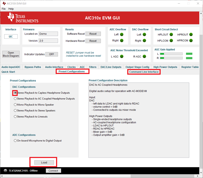
有一个文档《 TLV320AIC3104编程更加轻松 》、我将其用作参考。 它在本文档末尾列出了一个启动脚本。 我尝试参考这些内容以便让3105启动并运行。  

我将从一个简单的示例开始... 我想、让我"为左右 DAC 加电"、即页0x00寄存器0x25 (37)。 我正在进行硬件复位(将 RESET 下拉至低电平、然后变为高电平)。 然后我将执行软件复位(写入复位寄存器)。  

// hardware reset
  pinMode(RESET_PIN,OUTPUT); 
  digitalWrite(RESET_PIN,HIGH);delay(50); //not reset
  digitalWrite(RESET_PIN,LOW);delay(100);  //reset
    Serial.println("-----this should fail-----");
    writeRegister(wires, dev, Page_00, 0x01, 0b10000000); 
    Serial.println("-----now turning it back on-----");
  digitalWrite(RESET_PIN,HIGH);delay(50);//not reset
    Serial.println("-----Hardware reset complete-----");


	// reset to defaults                    
	writeRegister(wires, dev, Page_00, 0x01, 0b10000000); // Reset Module | 0b00010001 | 0x11
  	writeRegister(wires, dev, Page_00, 0x01, 0b00000000); // Reset Module | 0b00010001 | 0x11
    if (debugToSerialTLV320AIC3105) Serial.println("-- Software Reset Complete ---");
  // wait for device to initialize
	delay(50);  

  //TEST SIMPLE DAC ENABLE/DISABLE. 
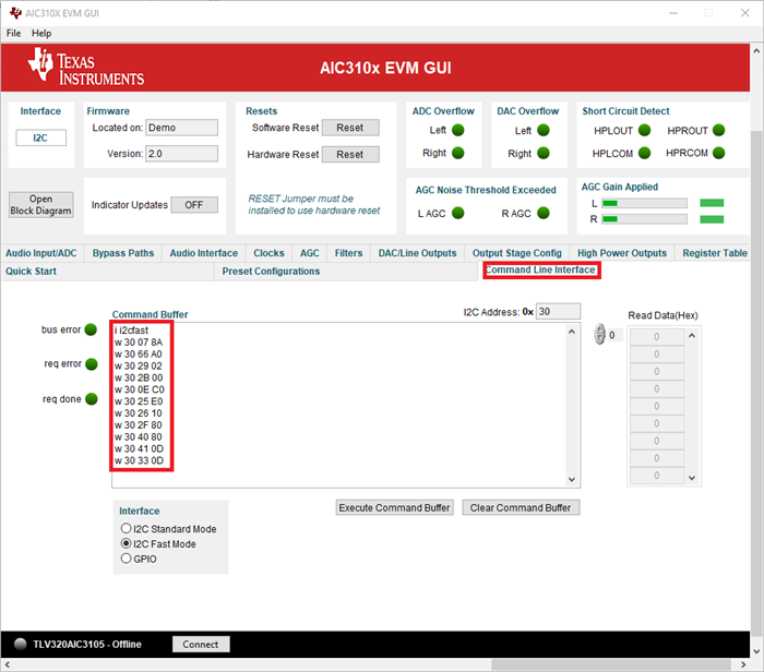
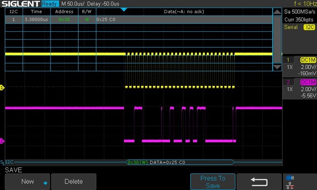
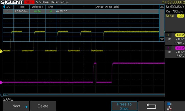
  writeRegister(wires, dev, Page_00, 37, 0b1110000);delay(50); // 
  writeRegister(wires, dev, Page_00, 38, 0b00010100);delay(50); //
    writeRegister(wires, dev, Page_00, 40, 0b11010101);delay(50); // 
dumpAllRegisters(wires, dev);

但是、当我运行代码时、结果不会"粘住"、这是不是为了让 I2C 设置在写入时粘住、我首先必须做些什么?

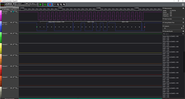
---Starting ----
Debugging to serial
AudioControlTLV320AIC3105::enableTLV320AIC3105
-----this should fail-----
controlTLV320AIC3105: Received Error During goToPage(): Error = 2
failed to transmit address
controlTLV320AIC3105: INFO: Read Page.  Page: 0 Reg: 1.  Failed to go to read page.  Could not go there.
Write:	 Wire:0	 TLV320AIC3105:24	 P0_R1	 P0x00_R0x1	 0x80	 128	 0b10000000
controlTLV320AIC3105: Received Error During goToPage(): Error = 2
failed to transmit address
controlTLV320AIC3105: Received Error During writePage(): Error = 2
-----now turning it back on-----
-----Hardware reset complete-----
Read:	 Wire:0	 TLV320AIC3105:24	 P0_R1	 P0x00_R0x1	 0x0	 0	 0b0
Write:	 Wire:0	 TLV320AIC3105:24	 P0_R1	 P0x00_R0x1	 0x80	 128	 0b10000000
Read:	 Wire:0	 TLV320AIC3105:24	 P0_R1	 P0x00_R0x1	 0x0	 0	 0b0

Read:	 Wire:0	 TLV320AIC3105:24	 P0_R1	 P0x00_R0x1	 0x0	 0	 0b0
Write:	 Wire:0	 TLV320AIC3105:24	 P0_R1	 P0x00_R0x1	 0x0	 0	 0b0
Read:	 Wire:0	 TLV320AIC3105:24	 P0_R1	 P0x00_R0x1	 0x0	 0	 0b0

-- Software Reset Complete ---
Read:	 Wire:0	 TLV320AIC3105:24	 P0_R37	 P0x00_R0x25	 0x0	 0	 0b0
Write:	 Wire:0	 TLV320AIC3105:24	 P0_R37	 P0x00_R0x25	 0x70	 112	 0b1110000
Read:	 Wire:0	 TLV320AIC3105:24	 P0_R37	 P0x00_R0x25	 0x0	 0	 0b0

Read:	 Wire:0	 TLV320AIC3105:24	 P0_R38	 P0x00_R0x26	 0x0	 0	 0b0
Write:	 Wire:0	 TLV320AIC3105:24	 P0_R38	 P0x00_R0x26	 0x14	 20	 0b10100
Read:	 Wire:0	 TLV320AIC3105:24	 P0_R38	 P0x00_R0x26	 0x0	 0	 0b0

Read:	 Wire:0	 TLV320AIC3105:24	 P0_R40	 P0x00_R0x28	 0x0	 0	 0b0
Write:	 Wire:0	 TLV320AIC3105:24	 P0_R40	 P0x00_R0x28	 0xD5	 213	 0b11010101
Read:	 Wire:0	 TLV320AIC3105:24	 P0_R40	 P0x00_R0x28	 0x0	 0	 0b0

初始化编解码器的基本步骤是什么? 很抱歉这里的基本问题,我已经与这个做了几天,我正在寻找一些帮助,希望得到这个移动. 谢谢!

  • 请注意,本文内容源自机器翻译,可能存在语法或其它翻译错误,仅供参考。如需获取准确内容,请参阅链接中的英语原文或自行翻译。

    您好、Jay、

    谢谢您的支持、我们很乐意为您提供帮助。  

    基本的启动序列是(1)对电源加电。 一旦所有电源稳定(2)、执行编解码器的软件复位。 此后、该器件能够通过 I2C 进行配置。 编解码器 GUI 有一个初始化脚本、此脚本也许是一个有用的资源。  

    通常、寄存器写入不"粘滞"的问题是器件未接收到有效的 I2C 读取/写入。 请探测 SDA 和 SDL、以确保总线具有来自主机控制器的有效 I2C 读取/写入。 您还可以读取初始值为非0的寄存器、例如 页0/寄存器58 (默认值为0x06)、以确保 I2C 正常工作。

    如果可能、还请共享正在使用的主机控制器和操作系统。

    让我知道结果。

    此致!
    Andrew

  • 请注意,本文内容源自机器翻译,可能存在语法或其它翻译错误,仅供参考。如需获取准确内容,请参阅链接中的英语原文或自行翻译。

    早上好!  

    我的项目有一个运行 TLV320AIC3105的 tensy 4.1。 我已完成大量测试、我可以确认 I2S 稳定、并且 I2C 正在控制该器件。  

    编解码器 GUI 的初始化脚本可能是一个有用的资源

    听起来正是我需要的。 我将尝试安装和使用它、我之前已将 GUI 用于其他项目。 我可以在没有 EVM 的情况下实现它吗? 您能给我发送一份脚本吗?

    杰伊

  • 请注意,本文内容源自机器翻译,可能存在语法或其它翻译错误,仅供参考。如需获取准确内容,请参阅链接中的英语原文或自行翻译。

    您好、Jay、

    是的、您可以在系统提示时选择"demo"来运行 GUI 而不使用 EVM。 在"Preset configuration"选项卡中选择所需的预设、然后选择"Load"脚本。 然后、将在"命令行界面"部分中生成脚本。 GUI 假设从 PAGE 0开始写入。 建议在 GUI 预设脚本中添加行以进行软件复位、并写入 PAGE 寄存器以确保初始条件(即 w 30 00 00 00)。


    使用预设脚本是一个很好的起点、您可以根据需要根据确切的用例来定制寄存器。 另请注意、对 GUI 的任何更改都将在命令行脚本中自动更新。

    如果您有任何其他问题、请告诉我。

    希望这对您有所帮助、
    好的

  • 请注意,本文内容源自机器翻译,可能存在语法或其它翻译错误,仅供参考。如需获取准确内容,请参阅链接中的英语原文或自行翻译。

    Andrew、您好!  

    该 GUI 工具比我使用的另一个工具好得多。 这很好,谢谢。  

    第一个问题是3105的地址。 GUI 工具尝试调用0x30的情况很奇怪、因为我在0x18上看到它、并且数据表显示"TLV320AIC3105响应 I2C 地址001 1000 "、即0b0011000 / 0x18 /或仅24作为十进制数。 这 有点让人困惑、您知道原因吗?

    我整理了这段代码、其中通过选择导线来指定 I2C 导线、将 DEV 设置为0x18表示地址、而 Page 仅为0x00。  

    //PRESET: 
    // DAC to Stereo Speakers
    
    // Digital audio setup for operation with AC-MODEVM
    
    // Input:
    // DAC
    //     - Left data to LDAC and right data to RDAC
    //     - Volume control = 0dB
    //     - Connected to outputs via mixer mode
    
    // Ouput:
    
    // High Power Outputs
    //     - Differential speaker outputs
    //     - LDAC to HPLOUT/COM
    //     - RDAC to HPROUT/COM
    //     - Mixer gain = 0dB
    //     - Output amplifier gain = 0dB
    
    writeRegister(wires, dev, Page_00, 0x07, 0x8A);// w 30 07 8A
    writeRegister(wires, dev, Page_00, 0x66, 0xA0);// w 30 66 A0
    writeRegister(wires, dev, Page_00, 0x25, 0xC0);// w 30 25 C0
    writeRegister(wires, dev, Page_00, 0x2B, 0x00);// w 30 2B 00
    writeRegister(wires, dev, Page_00, 0x29, 0x02);// w 30 29 02
    writeRegister(wires, dev, Page_00, 0x0E, 0xC0);// w 30 0E C0
    writeRegister(wires, dev, Page_00, 0x2F, 0x80);// w 30 2F 80
    writeRegister(wires, dev, Page_00, 0x40, 0x80);// w 30 40 80
    writeRegister(wires, dev, Page_00, 0x41, 0x0D);// w 30 41 0D
    writeRegister(wires, dev, Page_00, 0x33, 0x0D);// w 30 33 0D

    一切都运行良好,确认如下所示... 除了第0页的寄存器37、即"表42。 页0/寄存器37:DAC 功率和输出驱动器控制寄存器"。 这是为左右 DAC 加电的重要寄存器...  

    -----Hardware reset complete-----
    Read:	 Wire:0	 TLV320AIC3105:24	 P0_R1	 P0x00_R0x1	 0x0	 0	 0b0
    Write:	 Wire:0	 TLV320AIC3105:24	 P0_R1	 P0x00_R0x1	 0x1	 1	 0b1
    Read:	 Wire:0	 TLV320AIC3105:24	 P0_R1	 P0x00_R0x1	 0x1	 1	 0b1
    
    Read:	 Wire:0	 TLV320AIC3105:24	 P0_R1	 P0x00_R0x1	 0x1	 1	 0b1
    Write:	 Wire:0	 TLV320AIC3105:24	 P0_R1	 P0x00_R0x1	 0x0	 0	 0b0
    Read:	 Wire:0	 TLV320AIC3105:24	 P0_R1	 P0x00_R0x1	 0x0	 0	 0b0
    
    -- Software Reset Complete ---
    Read:	 Wire:0	 TLV320AIC3105:24	 P0_R7	 P0x00_R0x7	 0x0	 0	 0b0
    Write:	 Wire:0	 TLV320AIC3105:24	 P0_R7	 P0x00_R0x7	 0x8A	 138	 0b10001010
    Read:	 Wire:0	 TLV320AIC3105:24	 P0_R7	 P0x00_R0x7	 0x82	 130	 0b10000010
    
    Read:	 Wire:0	 TLV320AIC3105:24	 P0_R102	 P0x00_R0x66	 0x0	 0	 0b0
    Write:	 Wire:0	 TLV320AIC3105:24	 P0_R102	 P0x00_R0x66	 0xA0	 160	 0b10100000
    Read:	 Wire:0	 TLV320AIC3105:24	 P0_R102	 P0x00_R0x66	 0xA0	 160	 0b10100000
    
    Read:	 Wire:0	 TLV320AIC3105:24	 P0_R37	 P0x00_R0x25	 0x0	 0	 0b0
    Write:	 Wire:0	 TLV320AIC3105:24	 P0_R37	 P0x00_R0x25	 0xC0	 192	 0b11000000
    Read:	 Wire:0	 TLV320AIC3105:24	 P0_R37	 P0x00_R0x25	 0x0	 0	 0b0
    
    Read:	 Wire:0	 TLV320AIC3105:24	 P0_R43	 P0x00_R0x2B	 0x80	 128	 0b10000000
    Write:	 Wire:0	 TLV320AIC3105:24	 P0_R43	 P0x00_R0x2B	 0x0	 0	 0b0
    Read:	 Wire:0	 TLV320AIC3105:24	 P0_R43	 P0x00_R0x2B	 0x0	 0	 0b0
    
    Read:	 Wire:0	 TLV320AIC3105:24	 P0_R41	 P0x00_R0x29	 0x0	 0	 0b0
    Write:	 Wire:0	 TLV320AIC3105:24	 P0_R41	 P0x00_R0x29	 0x2	 2	 0b10
    Read:	 Wire:0	 TLV320AIC3105:24	 P0_R41	 P0x00_R0x29	 0x2	 2	 0b10
    
    Read:	 Wire:0	 TLV320AIC3105:24	 P0_R14	 P0x00_R0xE	 0x80	 128	 0b10000000
    Write:	 Wire:0	 TLV320AIC3105:24	 P0_R14	 P0x00_R0xE	 0xC0	 192	 0b11000000
    Read:	 Wire:0	 TLV320AIC3105:24	 P0_R14	 P0x00_R0xE	 0xC0	 192	 0b11000000
    
    Read:	 Wire:0	 TLV320AIC3105:24	 P0_R47	 P0x00_R0x2F	 0x0	 0	 0b0
    Write:	 Wire:0	 TLV320AIC3105:24	 P0_R47	 P0x00_R0x2F	 0x80	 128	 0b10000000
    Read:	 Wire:0	 TLV320AIC3105:24	 P0_R47	 P0x00_R0x2F	 0x80	 128	 0b10000000
    
    Read:	 Wire:0	 TLV320AIC3105:24	 P0_R64	 P0x00_R0x40	 0x4	 4	 0b100
    Write:	 Wire:0	 TLV320AIC3105:24	 P0_R64	 P0x00_R0x40	 0x80	 128	 0b10000000
    Read:	 Wire:0	 TLV320AIC3105:24	 P0_R64	 P0x00_R0x40	 0x80	 128	 0b10000000
    
    Read:	 Wire:0	 TLV320AIC3105:24	 P0_R65	 P0x00_R0x41	 0x0	 0	 0b0
    Write:	 Wire:0	 TLV320AIC3105:24	 P0_R65	 P0x00_R0x41	 0xD	 13	 0b1101
    Read:	 Wire:0	 TLV320AIC3105:24	 P0_R65	 P0x00_R0x41	 0xD	 13	 0b1101
    
    Read:	 Wire:0	 TLV320AIC3105:24	 P0_R51	 P0x00_R0x33	 0x0	 0	 0b0
    Write:	 Wire:0	 TLV320AIC3105:24	 P0_R51	 P0x00_R0x33	 0xD	 13	 0b1101
    Read:	 Wire:0	 TLV320AIC3105:24	 P0_R51	 P0x00_R0x33	 0xD	 13	 0b1101
    
    Table 96. Page 0/Register 96: Sticky Interrupt Flags Register
    Read:	 Wire:0	 TLV320AIC3105:24	 P0_R96	 P0x00_R0x60	 0x0	 0	 0b0
    AudioControlTLV320AIC3105::enableTLV320AIC3105
    
    ---Starting Audio Library----
    

    您是否有任何线索、我可以了解为何无法在 P0R37上为 DAC 加电? 我应该查看某个位置是否有一个旗帜、以便查看是否一切正常? 在启用 DAC 之前、是否可能缺少某些配置?

    再次感谢、

    杰伊

  • 请注意,本文内容源自机器翻译,可能存在语法或其它翻译错误,仅供参考。如需获取准确内容,请参阅链接中的英语原文或自行翻译。

    Joey、您好!

    奇怪的是 GUI 工具正在尝试调用0x30,因为我在0x18上看到它

    很抱歉、我应该在上一个帖子中指定了此内容。 您更正了仅器件本身的默认值为0x18。 EVM 和 GUI 使用 USB 转 I2C 接口、此器件的地址为0x30。  

    您是否有任何线索,我可以找到为什么我无法在 P0R37上启动 DAC?

    我建议在尝试写入  P0_R37时探测 I2C 总线。 如果命令未得到确认(NACK)、则 I2命令存在问题。 如果已确认(但仍未配置寄存器)、我们将进一步了解器件本身的详细信息。 您还可以配置 Table 105。 页0/寄存器107:新的可编程 ADC 数字路径和 I2C 总线条件寄存器、用于查看那里是否出现一个标志。

    状态寄存器页0/寄存器94和 页0/寄存器95也有助于进行检查。 这将显示器件的通电条件。

    在启用 DAC 之前是否缺少某些配置?

    一般而言、该配置和过程看起来不错。 此处需要进行一些调试才能找到根本原因。

    让我知道结果。

    -安德鲁

  • 请注意,本文内容源自机器翻译,可能存在语法或其它翻译错误,仅供参考。如需获取准确内容,请参阅链接中的英语原文或自行翻译。

    Andrew、您好!  

    感谢你的帮助。 我已经将器件连接到示波器并配置了解码。 似乎我将为该命令获得一个干净的信号。  

    // Table 42. Page 0/Register 37: DAC Power and Output Driver Control Register
    writeRegister(wires, dev, Page_00, 0x25, 0xC0);// w 30 25 C0

    但似乎我没有得到 ACK 吗?

    最后一位

    您也可以配置 Table 105。 页0/寄存器107:新的可编程 ADC 数字路径和 I2C 总线条件寄存器、用于查看那里是否出现一个标志。

    我在运行命令后运行该标志、但未收到任何标志(0x00)。

    Read:	 Wire:1	 TLV320AIC3105:24	 P0_R107	 P0x00_R0x6B	 Value: 0x0	 0	 0b0

    我运行了其他标志、唯一值得注意的结果是 DAC 未通电(寄存器94应显示1101100)。

    Table 94. Page 0/Register 94: Module Power Status Register
    Read:	 Wire:1	 TLV320AIC3105:24	 P0_R94	 P0x00_R0x5E	 Value: 0xC	 12	 0b1100
    Table 95. Page 0/Register 95: Output Driver Short-Circuit Detection Status Register
    Read:	 Wire:1	 TLV320AIC3105:24	 P0_R95	 P0x00_R0x5F	 Value: 0x0	 0	 0b0
    Table 96. Page 0/Register 96: Sticky Interrupt Flags Register
    Read:	 Wire:1	 TLV320AIC3105:24	 P0_R96	 P0x00_R0x60	 Value: 0x0	 0	 0b0

    我有一点好奇、为什么除了 DAC 配置之外、很多命令似乎都成功-即使没有确认也是如此。

    地址显示为0x30。 我不确定该部件与7位与8位地址有关。 但设备显然是响应命令,只是不是 ACK...  

    我有点困惑。 对我来说、信号没问题、您看到我缺少什么吗?

    杰伊

  • 请注意,本文内容源自机器翻译,可能存在语法或其它翻译错误,仅供参考。如需获取准确内容,请参阅链接中的英语原文或自行翻译。

    我还用逻辑分析仪记录了这些步骤、我实际上似乎获得了 ACK。 看起来不错、只是 P0R37写入没有粘滞。  

    Time[s],Packet ID,Address,Read/Write,Data
    0.0000000000,1,0x30,Write,0x00 0x00
    0.0302882900,2,0x30,Write,0x01 0x01
    1.2305965200,3,0x30,Write,0x00 0x00
    1.2608848200,4,0x30,Write,0x01 0x00
    2.5111936700,5,0x30,Write,0x00 0x00
    2.5414812300,6,0x30,Write,0x07 0x8A
    2.7417776800,7,0x30,Write,0x00 0x00
    2.7720650700,8,0x30,Write,0x66 0xA0
    2.9723606900,9,0x30,Write,0x00 0x00
    3.0026489900,10,0x30,Write,0x25 0xC0
    3.2029445300,11,0x30,Write,0x00 0x00
    3.2332318300,12,0x30,Write,0x2B 0x00
    3.4335275300,13,0x30,Write,0x00 0x00
    3.4638157600,14,0x30,Write,0x29 0x02
    3.6641113800,15,0x30,Write,0x00 0x00
    3.6943996800,16,0x30,Write,0x0E 0xC0
    3.8946953900,17,0x30,Write,0x00 0x00
    3.9249836800,18,0x30,Write,0x2F 0x80
    4.1252792200,19,0x30,Write,0x00 0x00
    4.1555666100,20,0x30,Write,0x40 0x80
    4.3558620700,21,0x30,Write,0x00 0x00
    4.3861504500,22,0x30,Write,0x41 0x0D
    4.5864460700,23,0x30,Write,0x00 0x00
    4.6167343800,24,0x30,Write,0x33 0x0D
    4.8170300800,25,0x30,Write,0x00 0x00
    4.8473183800,26,0x30,Write,0x25 0xC0
    5.1476101100,27,0x30,Write,0x00 0x00
    5.3478996400,28,0x30,Write,0x6B
    5.4480980000,29,0x31,Read,0x00
    5.8483059900,30,0x30,Write,0x00 0x00
    6.0485957000,31,0x30,Write,0x5E
    6.1487948900,32,0x31,Read,0x0C
    6.5490029600,33,0x30,Write,0x00 0x00
    6.7492935000,34,0x30,Write,0x5F
    6.8494928500,35,0x31,Read,0x00
    7.2497008400,36,0x30,Write,0x00 0x00
    7.4499903000,37,0x30,Write,0x60
    7.5501886500,38,0x31,Read,0x00

    更新:我插入了耳机、听到扬声器发出声音! 这种情况发生在程序上载一个分裂的第二-所以这是个好消息。 我只需要弄清楚它为什么不可靠。 我显然在那里。  

  • 请注意,本文内容源自机器翻译,可能存在语法或其它翻译错误,仅供参考。如需获取准确内容,请参阅链接中的英语原文或自行翻译。

    您好、Jay、  

    我同意这是一个奇怪的问题。 您似乎采取了所有正确的步骤。

    几个问题(如下所示):

    1. 您是否在使用 TLV320AIC3105EVM 或者这些 I2C 写入是否在定制 PCB 上?
      1. 如果使用 EVM、您在使用哪种主板? (USB MOD 接口或 AC-MODEVM)。 此时、您的测试设置图片可能会有所帮助。
    2. 我注意到您的最后一个脚本写入了0x30、从0x31读取。 这有什么用呢? 从正面值看、这表示您正在读取不同器件的寄存器。 我不认为这是你以前的帖子的情况。  
    3. 驱动器上电后、两个寄存器0x25是否进行任何写入?

    此致!
    Andrew

  • 请注意,本文内容源自机器翻译,可能存在语法或其它翻译错误,仅供参考。如需获取准确内容,请参阅链接中的英语原文或自行翻译。

    Andrew、您好!  

    • 您是否在使用 TLV320AIC3105EVM 或者这些 I2C 写入是否在定制 PCB 上?
      1. 如果使用 EVM、您在使用哪种主板? (USB MOD 接口或 AC-MODEVM)。 此时、您的测试设置图片可能会有所帮助。
    [/报价]

    这是定制 PCB。 如果可以、我可以在 PM 中分享照片。 现在、我想让它成为一个惊喜。 :-)

    • 我注意到您的最后一个脚本写入了0x30、从0x31读取。 这有什么用呢? 从正面值看、这表示您正在读取不同器件的寄存器。 我不认为这是你以前的帖子的情况。  
    [/报价]

    分析仪上显示的0x30表示写入、0x31表示读取... !? 我认为这与7位到8位寻址有关。 实际上、这可能是 USB EVM 预期的内容、完整的8位地址。 我很抱歉我现在还没有其他想法,因为我还在学习。 但可以说、我100%与器件通信、现在可以可靠地进行读取和写入。  

    我能够使一切正常工作、包括播放和录制路径。  我还有其他工作要做,但就基本操作而言,我让它在您的帮助下工作。 谢谢!

    [/quote]
  • 请注意,本文内容源自机器翻译,可能存在语法或其它翻译错误,仅供参考。如需获取准确内容,请参阅链接中的英语原文或自行翻译。

    您好、Jay、

    我很高兴听到您的应用现在正在工作。 感谢您为您解释了修复问题的方式(并将帖子标记为已解决)。 我觉得 EVM 需要一个完整的8位地址 、因为  EVM 和 GUI 使用外部 USB 转 I2C 接口。 所以这是一个很好的发现。  

    如果您有其他问题、请随时打开另一个主题。

    此致!
    Andrew