请注意,本文内容源自机器翻译,可能存在语法或其它翻译错误,仅供参考。如需获取准确内容,请参阅链接中的英语原文或自行翻译。
部件号:TMS320F2.8388万D 主题中讨论的其他部件: C2000WARE
我们有一个带有两个TMS320F2.8388万D处理器的定制板。 我能够连接到处理器,并可以运行和调试从RAM正常运行的小应用程序。 我们的程序已经发展到比为RAM分配的空间更大,所以现在我尝试从闪存中运行应用程序。
我有一个非常小的盲项目,可以从RAM运行,但一旦我从闪存运行它,我就会遇到问题。
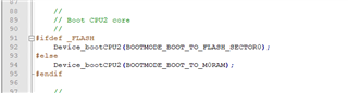
在JTAG链中的第一个处理器上加载到闪存的同一项目可以从RAM和闪存中正常运行/调试。 第二个只能从RAM进行调试。 我可以通过启动下面的目标配置正常闪烁(启动时LED开始闪烁),
连接目标

加载程序。 然后我得到以下调试输出
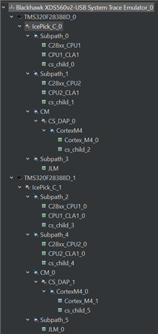
C28xx_CPU1_0: GEL Output:
Memory Map Initialization Complete
C28xx_CPU1_0: GEL Output:
... DCSM Initialization Start ...
C28xx_CPU1_0: GEL Output:
... DCSM Initialization Done ...
C28xx_CPU1_0: GEL Output:
 CPU2 is out of reset and configured to wait boot.
 (If you connected previously, may have to resume CPU2 to reach wait boot loop.)
C28xx_CPU1_0: GEL Output:
 CM is out of reset and configured to wait boot.
 (If you connected previously, may have to resume CM to reach wait boot loop.)
C28xx_CPU1_0: If erase/program (E/P) operation is being done on one core, the other core should not execute from shared-RAM (SR) as they are used for the E/P code. User code execution from SR could commence after both flash banks are programmed.
C28xx_CPU1_0: Only CPU1 on-chip Flash Plugin can configure clock for CPU1, CPU2 and CM Flash operations. Plugin automatically configures PLL when CPU1 Flash operations are invoked. However, if users want to do only CPU2 or CM Flash operations without doing a prior CPU1 operation in the current session, they should click on 'Configure Clock' button in CPU1's on-chip Flash Plugin before invoking CPU2 and CM Flash operations. When this button is used, Flash Plugin will configure the clock for CPU1/CPU2 at 190MHz and CM at 95MHz using INTOSC2 as the clock source. Plugin will leave PLL config like this and user application should configure the PLL as required by application.
C28xx_CPU1_0: GEL Output:
... DCSM Initialization Start ...
C28xx_CPU1_0: GEL Output:
... DCSM Initialization Done ...
C28xx_CPU1_0: GEL Output:
 CPU2 is out of reset and configured to wait boot.
 (If you connected previously, may have to resume CPU2 to reach wait boot loop.)
C28xx_CPU1_0: GEL Output:
 CM is out of reset and configured to wait boot.
 (If you connected previously, may have to resume CM to reach wait boot loop.)
C28xx_CPU1_0: Writing Flash @ Address 0x00080000 of Length 0x00000002 (page 0)
C28xx_CPU1_0: GEL Output:
... DCSM Initialization Start ...
C28xx_CPU1_0: GEL Output:
... DCSM Initialization Done ...
C28xx_CPU1_0: GEL Output:
 CPU2 is out of reset and configured to wait boot.
 (If you connected previously, may have to resume CPU2 to reach wait boot loop.)
C28xx_CPU1_0: GEL Output:
 CM is out of reset and configured to wait boot.
 (If you connected previously, may have to resume CM to reach wait boot loop.)
C28xx_CPU1_0: PLL configuration status = 1. PLL configured successfully.
C28xx_CPU1_0: Erasing Flash Bank 0, Sector 0
C28xx_CPU1_0: Erasing Flash Bank 0, Sector 1
C28xx_CPU1_0: Erasing Flash Bank 0, Sector 2
C28xx_CPU1_0: Erasing Flash Bank 0, Sector 3
C28xx_CPU1_0: Erasing Flash Bank 0, Sector 4
C28xx_CPU1_0: Erasing Flash Bank 0, Sector 5
C28xx_CPU1_0: Erasing Flash Bank 0, Sector 6
C28xx_CPU1_0: Erasing Flash Bank 0, Sector 7
C28xx_CPU1_0: Erasing Flash Bank 0, Sector 8
C28xx_CPU1_0: Erasing Flash Bank 0, Sector 9
C28xx_CPU1_0: Erasing Flash Bank 0, Sector 10
C28xx_CPU1_0: Erasing Flash Bank 0, Sector 11
C28xx_CPU1_0: Erasing Flash Bank 0, Sector 12
C28xx_CPU1_0: Erasing Flash Bank 0, Sector 13
C28xx_CPU1_0: Data has been buffered at the end of the current data block for 64-bit aligned writes.
C28xx_CPU1_0: Writing Flash @ Address 0x00082000 of Length 0x00000fdf (page 0)
C28xx_CPU1_0: Data has been buffered at the end of the current data block for 64-bit aligned writes.
C28xx_CPU1_0: --Verifying Flash @ Address 0x00082000 of Length 0x00000FDC
C28xx_CPU1_0: Writing Flash @ Address 0x00086000 of Length 0x0000012d (page 0)
C28xx_CPU1_0: Data has been buffered at the end of the current data block for 64-bit aligned writes.
C28xx_CPU1_0: --Verifying Flash @ Address 0x00086000 of Length 0x0000012C
C28xx_CPU1_0: Writing Flash @ Address 0x00088000 of Length 0x00000014 (page 0)
C28xx_CPU1_0: --Verifying Flash @ Address 0x00088000 of Length 0x00000014
C28xx_CPU1_0: Writing Flash @ Address 0x00090000 of Length 0x000002f5 (page 0)
C28xx_CPU1_0: Data has been buffered at the end of the current data block for 64-bit aligned writes.
C28xx_CPU1_0: --Verifying Flash @ Address 0x00090000 of Length 0x000002F4
C28xx_CPU1_0: Writing buffered data @ Address 0x00080000 of Length 0x00000004
C28xx_CPU1_0: --Verifying Flash @ Address 0x00080000 of Length 0x00000004
C28xx_CPU1_0: Writing buffered data @ Address 0x00082FDC of Length 0x00000004
C28xx_CPU1_0: --Verifying Flash @ Address 0x00082FDC of Length 0x00000004
C28xx_CPU1_0: Writing buffered data @ Address 0x0008612C of Length 0x00000004
C28xx_CPU1_0: --Verifying Flash @ Address 0x0008612C of Length 0x00000004
C28xx_CPU1_0: Writing buffered data @ Address 0x000902F4 of Length 0x00000004
C28xx_CPU1_0: --Verifying Flash @ Address 0x000902F4 of Length 0x00000004
C28xx_CPU1_0: Trouble Setting Breakpoint with the Action "Finish Auto Run" at 0x82ed4: (Error -1066 @ 0x82ED4) Unable to set/clear requested breakpoint. Verify that the breakpoint address is in valid memory. (Emulation package 9.6.0.00172)
最后一个部分是我一直被卡住的地方。 是否有地方需要指定起始位置或断点地址,因为它位于处理器2上?
我正在使用CCS 11.1 .........0
谢谢你