请注意,本文内容源自机器翻译,可能存在语法或其它翻译错误,仅供参考。如需获取准确内容,请参阅链接中的英语原文或自行翻译。
器件型号:TMS320F28335 主题中讨论的其他器件:UNIFLASH、 C2000WARE
您好!
我关注的是我在 https://e2e.ti.com/support/microcontrollers/c2000-microcontrollers-group/c2000/f/c2000-microcontrollers-forum/1225088/tms320f28335-cpu-is-not-running-after-power-off-on-but-it-runs-after-flash-load/4665801上的这个问题、该问题已关闭、但我没有解决我的问题。 因此、这里存在互补问题。
基本上、在关闭/打开 DSP 的电源之后、DSP 未运行、但它在使用 Uniflash 加载程序之后运行。
在 MatthewRate 提出的最后一个问题后、以下是我在调试中发现的问题:
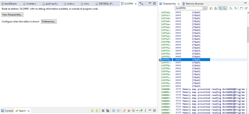
CPU 复位后、我的程序在这里等待:

然后、在运行和停止之后、它被锁定在这里:

(在程序之外)。
我试图在未执行复位的情况下解决调试会话、程序首先在这里等待:

然后它会按预期工作。
感谢所有可以帮助我的人。
祝您愉快!
最棒的酒店
马特奥