Other Parts Discussed in Thread: ADS8326, C2000WARE, CONTROLSUITE
主题中讨论的其他器件:ADS8326、 C2000WARE、 controlSUITE
您好!
我是 F28027的初学者、现在我正在尝试配置 SCI。 我已经成功地将器件配置为9600波特、但无法将 其增加到115200。
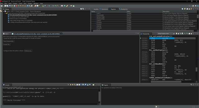
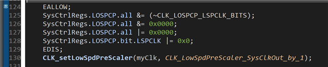
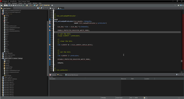
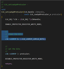
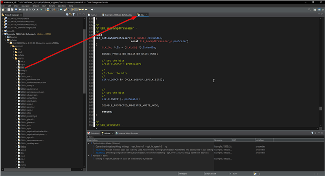
首先、我将低速时钟预分频器(LOSPCP)设置为/1。
CLK_setLowSpdPreScaler(myClk, CLK_LowSpdPreScaler_SysClkOut_by_1);
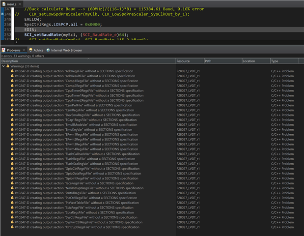
接下来、我设置 BRR 寄存器值、我计算如下:
BRR =(60MHz /(115200* 8))-1 = 64.10 ~ 64
反向计算波特-->(60MHz)/((16+1)* 8)= 115384.61波特、0.16%误差
SCI_setBaudRate(mySci, (SCI_BaudRate_e)64);
当我打开终端时、传输是一组随机字符。
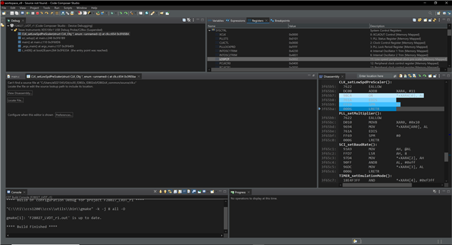
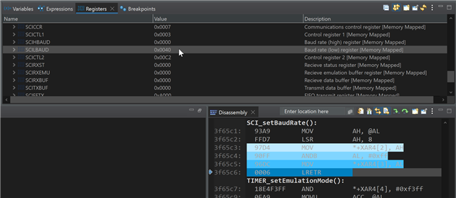
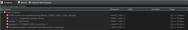
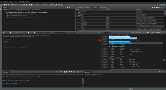
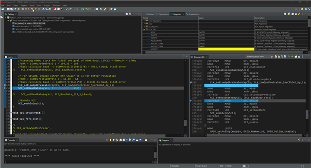
我仔细检查了寄存器、发现 BRR 正在按预期更新、但 LOSPCP 没有在默认值0x0002基础上发生变化。 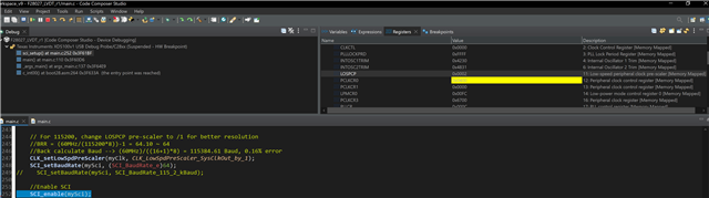
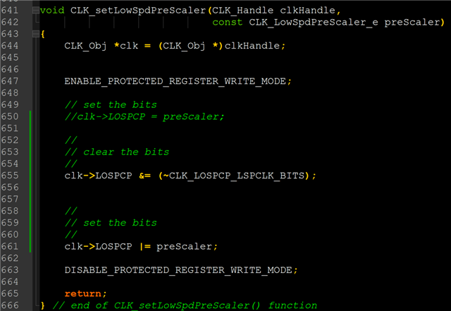
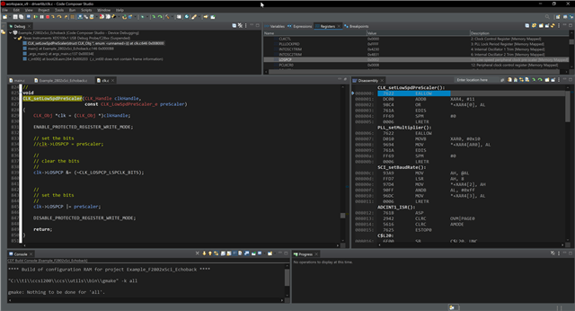
我正在使用 CLK_setLowSpdPreScaler()函数,但似乎没有效果。 我查看了 clk.c 文件、它看起来处理 EALLOW 和 EDIS、所以我假设这不是问题。
为了修改 LOSPCP、是否需要更改或设置其他内容? 很抱歉、这是一个基本问题、但除了需要设置 EALLOW 外、我还难以在参考手册中找到有关更改此寄存器的信息。
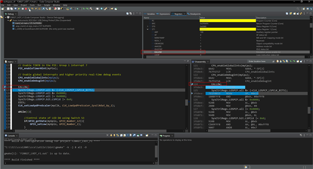
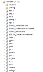
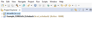
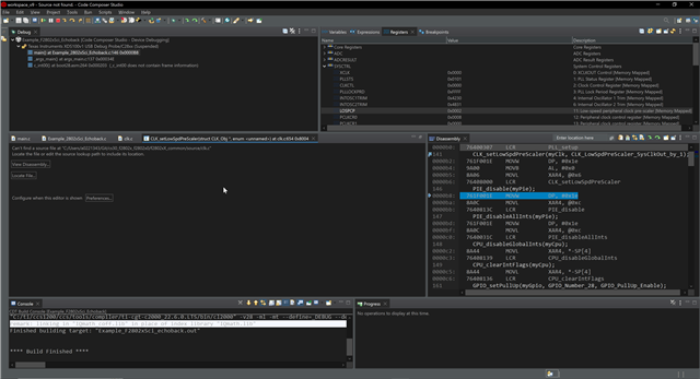
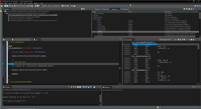
下面是该项目的屏幕截图:
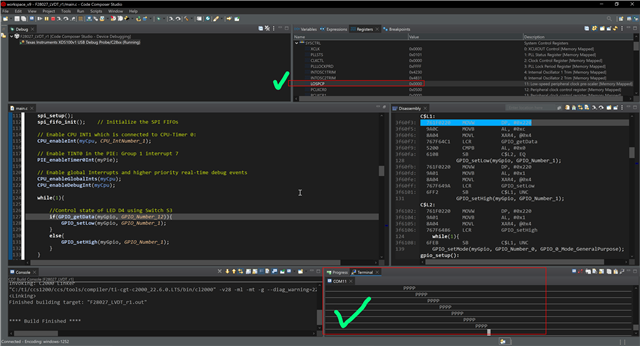
这是我的 main.c :
#include "DSP28x_Project.h" // Device Headerfile and Examples Include File (includes stdint.h)
// Include driver header files#include "f2802x_common/include/adc.h"#include "f2802x_common/include/clk.h"#include "f2802x_common/include/gpio.h"#include "f2802x_common/include/pie.h"#include "f2802x_common/include/pll.h"#include "f2802x_common/include/timer.h"#include "f2802x_common/include/wdog.h"#include "f2802x_common/include/sci.h"#include "f2802x_common/include/spi.h"
// Declare function prototype__interrupt void cpu_timer0_isr(void);void gpio_setup(void);void sci_setup(void);void spi_setup(void);void spi_fifo_init(void);
// Declare HandlesADC_Handle myAdc;CLK_Handle myClk;GPIO_Handle myGpio;PIE_Handle myPie;TIMER_Handle myTimer;SCI_Handle mySci;SPI_Handle mySpi;
int main(void){ // Declare local handles CPU_Handle myCpu; WDOG_Handle myWDog; PLL_Handle myPll;
// Initialize handles myAdc = ADC_init((void *)ADC_BASE_ADDR, sizeof(ADC_Obj)); myClk = CLK_init((void *)CLK_BASE_ADDR, sizeof(CLK_Obj)); myCpu = CPU_init((void *)NULL, sizeof(CPU_Obj)); myGpio = GPIO_init((void *)GPIO_BASE_ADDR, sizeof(GPIO_Obj)); myPie = PIE_init((void *)PIE_BASE_ADDR, sizeof(PIE_Obj)); myPll = PLL_init((void *)PLL_BASE_ADDR, sizeof(PLL_Obj)); myTimer = TIMER_init((void *)TIMER0_BASE_ADDR, sizeof(TIMER_Obj)); myWDog = WDOG_init((void *)WDOG_BASE_ADDR, sizeof(WDOG_Obj)); mySci = SCI_init((void *)SCIA_BASE_ADDR,sizeof(SCI_Obj)); mySpi = SPI_init((void *)SPIA_BASE_ADDR, sizeof(SPI_Obj));
// Initialize watchdog handle and disable. myWDog = WDOG_init((void *)WDOG_BASE_ADDR, sizeof(WDOG_Obj)); WDOG_disable(myWDog);
// Load oscillator calibration values using Device_cal // According to TRM section 1.3.2.1.2, ADC clocks must be enabled to calibrate the oscillators and ADC parameters. CLK_enableAdcClock(myClk); (*Device_cal)(); CLK_disableAdcClock(myClk); //Since the ADC is not needed for this application, it is disabled once calibration is done.
// Set internal oscillator 1 as the clock source. CLK_setOscSrc(myClk, CLK_OscSrc_Internal);
// Internal oscillator 1 runs at 10MHz, I need 60MHz. Multiply 10MHz by 12, divide by 2 PLL_setup(myPll, PLL_Multiplier_12, PLL_DivideSelect_ClkIn_by_2);
//Disable PIE and all interrupts before changing PIE PIE_disable(myPie); PIE_disableAllInts(myPie); CPU_disableGlobalInts(myCpu); CPU_clearIntFlags(myCpu);
// Re-enable PIE PIE_enable(myPie);
// Register interrupt handlers in the PIE vector table // Group number and subgroup number from TRM Table 1-110. PIE_registerPieIntHandler(myPie, PIE_GroupNumber_1, PIE_SubGroupNumber_7, (intVec_t)&cpu_timer0_isr);
#ifdef _FLASH memcpy(&RamfuncsRunStart, &RamfuncsLoadStart, (size_t)&RamfuncsLoadSize);#endif
// Configure CPU-Timer 0 to interrupt every 100 milliseconds: // 60MHz CPU Frequency TIMER_stop(myTimer); TIMER_setPeriod(myTimer, (uint32_t)(60 * 100000)); TIMER_setPreScaler(myTimer, 0); TIMER_reload(myTimer); TIMER_setEmulationMode(myTimer, TIMER_EmulationMode_StopAfterNextDecrement); //Note this is the default. TIMER_enableInt(myTimer);
TIMER_start(myTimer);
//Initialize GPIO gpio_setup();
//Set up SCIA sci_setup();
//Set up SPI spi_setup(); spi_fifo_init(); // Initialize the SPI FIFOs
// Enable CPU INT1 which is connected to CPU-Timer 0: CPU_enableInt(myCpu, CPU_IntNumber_1);
// Enable TINT0 in the PIE: Group 1 interrupt 7 PIE_enableTimer0Int(myPie);
// Enable global Interrupts and higher priority real-time debug events CPU_enableGlobalInts(myCpu); CPU_enableDebugInt(myCpu);
while(1){
//Control state of LED D4 using Switch S3 if(GPIO_getData(myGpio, GPIO_Number_12)){ GPIO_setLow(myGpio, GPIO_Number_1); } else{ GPIO_setHigh(myGpio, GPIO_Number_1); } }
}
void gpio_setup(void){ //LED D2 is connected to GPIO0. Set GPIO0 to GPIO configuration, output direction, and disable pull-up. GPIO_setMode(myGpio, GPIO_Number_0, GPIO_0_Mode_GeneralPurpose); GPIO_setDirection(myGpio, GPIO_Number_0, GPIO_Direction_Output); GPIO_setPullUp(myGpio, GPIO_Number_0, GPIO_PullUp_Disable); GPIO_setHigh(myGpio, GPIO_Number_0); //Initialize GPIO0 to known state
//LED D4 is connected to GPIO1. Set GPIO1 to GPIO configuration, output direction, and disable pull-up. GPIO_setMode(myGpio, GPIO_Number_1, GPIO_0_Mode_GeneralPurpose); GPIO_setDirection(myGpio, GPIO_Number_1, GPIO_Direction_Output); GPIO_setPullUp(myGpio, GPIO_Number_1, GPIO_PullUp_Disable); GPIO_setHigh(myGpio, GPIO_Number_1); //Initialize GPIO0 to known state
//LED D3 is connected to GPIO2. GPIO_setMode(myGpio, GPIO_Number_2, GPIO_0_Mode_GeneralPurpose); GPIO_setDirection(myGpio, GPIO_Number_2, GPIO_Direction_Output); GPIO_setPullUp(myGpio, GPIO_Number_2, GPIO_PullUp_Disable); GPIO_setHigh(myGpio, GPIO_Number_2); //Initialize GPIO0 to known state
//Switch S3 is connected to GPIO12. Set GPIO12 to GPIO configuration, input direction, and disable pull-up. GPIO_setMode(myGpio, GPIO_Number_12, GPIO_0_Mode_GeneralPurpose); GPIO_setDirection(myGpio, GPIO_Number_12, GPIO_Direction_Input); GPIO_setPullUp(myGpio, GPIO_Number_12, GPIO_PullUp_Disable);}
__interrupt void cpu_timer0_isr(void){ uint16_t txData16 = 0xFFFF; uint16_t adcData = 0x0000; uint16_t rxData1 = 0x0000; uint16_t rxData2 = 0x0000; //int i = 0;
//Set GPIO0 for debugging/LED GPIO_setHigh(myGpio, GPIO_Number_0);
//SPI Transmit two 16 bit words to TX FIFO SPI_write(mySpi,txData16); SPI_write(mySpi,txData16);
//Wait for 2 words to arrive while(SPI_getRxFifoStatus(mySpi) != SPI_FifoStatus_2_Words) { }
//SPI Read two 16 bit words from RX FIFO rxData1 = SPI_read(mySpi); rxData2 = SPI_read(mySpi);
//Combine rxData; discard first 6 adcData = ((rxData1 << 6) & 0xFFC0) | ((rxData2 >> 10) & 0x003F);
//UART Transmit //Send 16 bit integer as 4 4-bit integers ( //Terminate with line feed "\n" SCI_putDataBlocking(mySci, (uint8_t)(((adcData & 0xF000) >> 12) + 0x41)); SCI_putDataBlocking(mySci, (uint8_t)(((adcData & 0x0F00) >> 8) + 0x41)); SCI_putDataBlocking(mySci, (uint8_t)(((adcData & 0x00F0) >> 4) + 0x41)); SCI_putDataBlocking(mySci, (uint8_t)(((adcData & 0x000F) >> 0) + 0x41)); SCI_putDataBlocking(mySci, 0x0A); //LF
//Acknowledge interrupt so more interrupts from group 1 can be received. PIE_clearInt(myPie, PIE_GroupNumber_1);
//Set GPIO0 GPIO_setLow(myGpio, GPIO_Number_0);}
void sci_setup(void){ //See Example_2802xSci_FFDLB_int.c and TRM section 9.4 for configuration instructions GPIO_setPullUp(myGpio,GPIO_Number_28,GPIO_PullUp_Enable); GPIO_setPullUp(myGpio,GPIO_Number_29,GPIO_PullUp_Disable); GPIO_setQualification(myGpio,GPIO_Number_28,GPIO_Qual_ASync); GPIO_setMode(myGpio,GPIO_Number_28,GPIO_28_Mode_SCIRXDA); GPIO_setMode(myGpio,GPIO_Number_29,GPIO_29_Mode_SCITXDA);
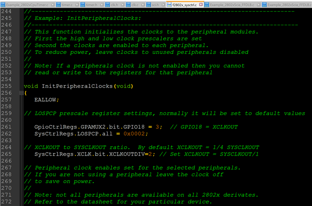
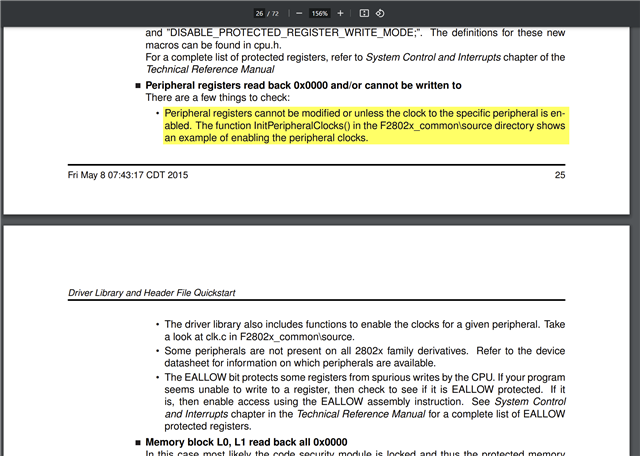
//Peripheral registers cannot be modified unless clock to the specific peripheral is enabled. //Source: Firmware Dev. Package User's Guide, section 2.6. //Enable clock to SCIA CLK_enableSciaClock(myClk);
//Set UART Settings. Parity disabled by default. SCI_disableParity(mySci); SCI_setNumStopBits(mySci, SCI_NumStopBits_One); SCI_setCharLength(mySci, SCI_CharLength_8_Bits);
//Enable Rx, Tx, Rx interrupt, Tx interrupt SCI_enableTx(mySci); SCI_enableRx(mySci); //SCI_enableTxInt(mySci); //Not needed. SCI_enableRxInt(mySci);
//Disable loopback SCI_disableLoopBack(mySci);
//RX ERR, Sleep, and TXWAKE are disabled by default after system reset.
//Set Baud Rate //Clock for SCI comes from LSPCLK, which is just SYSCLKOUT divided down according to LOSPCP register, default /4. //LSPCLK = SYSCLKOUT/(LOSPCP*2) . If LOSPCP = 0, LSPCLK = SYSCLKOUT //Baud rate = LSPCLK / ((BRR+1)*8), or inverse BRR = (LSPCLK/(Baud*8))-1 //BRR is the 16 bit value stored across SCIHBAUD and SCILBAUD // SCI BRR = LSPCLK/(SCI BAUDx8) - 1
//Assuming 60MHz clock for F28027 and goal of 9600 Baud, LSPCLK = 60MHz/4 = 15MHz //BRR = (15MHz/(9600*8))-1 = 194.31 ~ 194 //Back calculate Baud --> (60MHz/4)/((194+1)*8) = 9615.3 Baud, 0.16% error// SCI_setBaudRate(mySci, (SCI_BaudRate_e)194);
// For 115200, change LOSPCP pre-scaler to /1 for better resolution //BRR = (60MHz/(115200*8))-1 = 64.10 ~ 64 //Back calculate Baud --> (60MHz)/((16+1)*8) = 115384.61 Baud, 0.16% error CLK_setLowSpdPreScaler(myClk, CLK_LowSpdPreScaler_SysClkOut_by_1); SCI_setBaudRate(mySci, (SCI_BaudRate_e)64);
//Enable SCI SCI_enable(mySci);}
void spi_setup(void){ // Initialize GPIO for SPI GPIO_setPullUp(myGpio, GPIO_Number_16, GPIO_PullUp_Enable); GPIO_setPullUp(myGpio, GPIO_Number_17, GPIO_PullUp_Enable); GPIO_setPullUp(myGpio, GPIO_Number_18, GPIO_PullUp_Enable); GPIO_setPullUp(myGpio, GPIO_Number_19, GPIO_PullUp_Enable); GPIO_setQualification(myGpio, GPIO_Number_16, GPIO_Qual_ASync); //See TRM 1.4.4.1, SPI peripheral controls synchronization. GPIO_setQualification(myGpio, GPIO_Number_17, GPIO_Qual_ASync); GPIO_setQualification(myGpio, GPIO_Number_18, GPIO_Qual_ASync); GPIO_setQualification(myGpio, GPIO_Number_19, GPIO_Qual_ASync); GPIO_setMode(myGpio, GPIO_Number_16, GPIO_16_Mode_SPISIMOA); GPIO_setMode(myGpio, GPIO_Number_17, GPIO_17_Mode_SPISOMIA); GPIO_setMode(myGpio, GPIO_Number_18, GPIO_18_Mode_SPICLKA); GPIO_setMode(myGpio, GPIO_Number_19, GPIO_19_Mode_SPISTEA_NOT);
// Set GPIO 32 and 33 to inputs because they are jumped by traces to GPIO 16 and 17 //32 and 33 default to GPIO (see GPBMUX1 register), input direction (GPBDIR), enabled pull-up (GPBPUD).
//Enable clock first to allow change of configuration registers. CLK_enableSpiaClock(myClk);
//Set SPISWRESET bit, as directed by TRM 8.4.2 //This will also clear the OVERRUN_FLAG and INT_FLAG bits SPI_reset(mySpi);
// Enable master mode SPI_setMode(mySpi, SPI_Mode_Master); SPI_enableTx(mySpi);
//ADC is TI ADS8326, positive edge for DOUT SPI_setClkPhase(mySpi, SPI_ClkPhase_Normal); SPI_setClkPolarity(mySpi, SPI_ClkPolarity_OutputFallingEdge_InputRisingEdge);
SPI_setBaudRate(mySpi, SPI_BaudRate_1_MBaud); //DIFFERENT VALUE MIGHT BE NEEDED SINCE ENUM ASSUMES 12.5MHz //ADC can handle 24kHz to 6MHz. 15/12 = 1.25MHz
// Set 16-bit char bits SPI_setCharLength(mySpi, SPI_CharLength_16_Bits);
// Release SPI from Reset SPI_enable(mySpi);
return;}
void spi_fifo_init(){ // Initialize SPI FIFO registers SPI_enableChannels(mySpi); SPI_enableFifoEnh(mySpi); SPI_resetTxFifo(mySpi); SPI_clearTxFifoInt(mySpi); SPI_resetRxFifo(mySpi); SPI_clearRxFifoInt(mySpi); SPI_setRxFifoIntLevel(mySpi, SPI_FifoLevel_4_Words);
}