This thread has been locked.

If you have a related question, please click the "Ask a related question" button in the top right corner. The newly created question will be automatically linked to this question.

[参考译文] CDCE925:Xin/CLK:VI @ 2.5V 和6 mA

Guru**** 2383410 points
Other Parts Discussed in Thread: CDCE913
请注意,本文内容源自机器翻译,可能存在语法或其它翻译错误,仅供参考。如需获取准确内容,请参阅链接中的英语原文或自行翻译。

https://e2e.ti.com/support/clock-timing-group/clock-and-timing/f/clock-timing-forum/1080420/cdce925-xin-clk-vi-2-5v-and-6-ma

部件号:CDCE925
“线程”中讨论的其它部件:CDCE913

尊敬的各位先生:

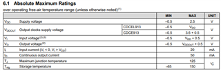
关于电压范围内的 CDCE913 CLK,我们错误地认为它与3.3V 兼容,如本主题所述:

  https://e2e.ti.com/support/clock-timing-group/clock-and-timing/f/clock-timing-forum/1075713/cdce925-clk-and-s0-pins-3-3v-compatibility?tisearch=e2e-quicksearch&keymatch=cdce913%20clk%20voltage

我们的问题是,哪些设计“强制”3.3V 超出串行电阻,并向 CLKIN 引脚输出6 mA 输入电流,这些电流稳定在2.5 V 左右,是否会随着时间的推移而失效?

现在,在发现这一点后,我们已经检查了 Vdd 电压1.8 V,并且稳定,因为据报道,Vdd 的消耗量为每 PLL ~9 mA。 来自该 CDCE 的抖动也符合规格要求。

当然,我们将通过适当的分隔符(源序列和目标并行)终止来纠正这一问题,以平衡线路。

此致,
乌鲁斯

  • 请注意,本文内容源自机器翻译,可能存在语法或其它翻译错误,仅供参考。如需获取准确内容,请参阅链接中的英语原文或自行翻译。

    关于 IBIS 模型(https://www.ti.com/lit/zip/scam056),它还定义了有效3.3V 范围的引脚:


    Model] clkin_0
    |
    |    Testbench Schematic clkin_0 model: Input
    |
    Model_type Input 
    |
    Vinl = 0.54   |--- Check this against the spec. 
    Vinh = 1.26   |--- Check this against the spec. 
    |
    | Variable       Typ                Min                Max 
    |
    C_comp       1.503583e-12       1.481523e-12       1.534573e-12
    |
    [Temperature range]      27              85              -40  
    [Voltage range]       3.300000             3.000000             3.600000  

  • 请注意,本文内容源自机器翻译,可能存在语法或其它翻译错误,仅供参考。如需获取准确内容,请参阅链接中的英语原文或自行翻译。

    你好,乌罗斯

    只要绝对最大规格未被违反,设备就不应随着时间的推移而损坏。  

    此致,