This thread has been locked.
If you have a related question, please click the "Ask a related question" button in the top right corner. The newly created question will be automatically linked to this question.
Other Parts Discussed in Thread: CDCDB803
https://e2e.ti.com/support/clock-timing-group/clock-and-timing/f/clock-timing-forum/1094248/cdcdb803-questions-about-the-clock-input-output-circuit-configuration-of-cdcdb803
您好,
我有关于cdcdb803的以下问题。
1.当3.3V电平CMOS单端信号用作输入时,CLKIN引脚的电路应如何配置?
2.当使用输出信号与LVDS兼容时,CK0~CK7输出引脚的电路应如何配置?
谢谢!
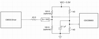
1. CDCDCDB803仅接受LP-HCSL输入。 要转换差动输入的CMOS信号,请使用以下端接。
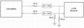
2. CDCDCDB803仅输出LP-HCSL输出。 要将输出转换为LVDS,请使用以下端接。
此致,
Kia Rahbar