This thread has been locked.

If you have a related question, please click the "Ask a related question" button in the top right corner. The newly created question will be automatically linked to this question.

[参考译文] DAC3162EVM:内部计时

Guru**** 657500 points
Other Parts Discussed in Thread: DAC3162
请注意,本文内容源自机器翻译,可能存在语法或其它翻译错误,仅供参考。如需获取准确内容,请参阅链接中的英语原文或自行翻译。

https://e2e.ti.com/support/data-converters-group/data-converters/f/data-converters-forum/1092710/dac3162evm-timing-with-internal-clocking

部件号:DAC3162EVM
主题中讨论的其他部件:DAC3162

大家好,寻求帮助。

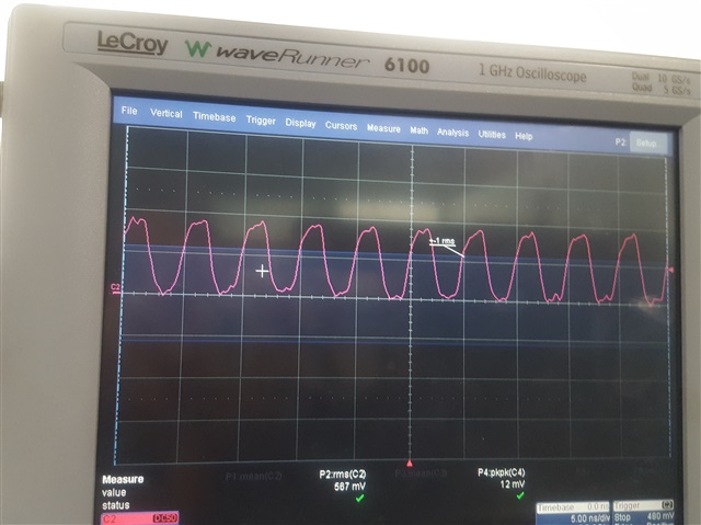
我尝试使用FPGA @ 200MHz驱动DAC3162。 DAC输入在每个时钟边缘从0x000切换到0xFFF,反之亦然,以检查全分辨率。
我尝试生成DAC数据(DDR格式),如图数据传输格式所示,并发送时钟信号200MHz,Vrms =0.56V
在附加的输入clk和测量的输出信号中(您也可以检查编入FPGA的FMC连接器的仿真信号)

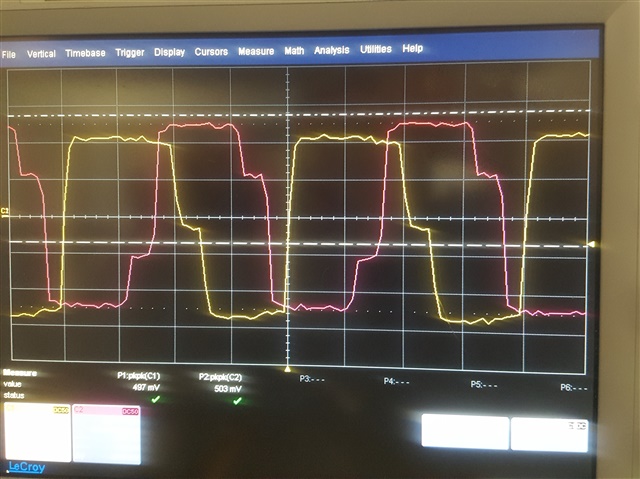
我需要任何建议来调整内部计时的时间。 如信息所示,DAC通过FPGA进行控制。 随附从DAC3162接收到的clk以及DAC的两个输出信号。

/resize-image/__size/640x480/__key/communityserver-discussionse-components_files/73/InputCLK_5F00_J9.jpg

/resize-image/__size/640x480/__key/communityserver-discussionse-components_files/73/waveform-_2800_1_2900_.png</s>2900

谢谢你。

标记