This thread has been locked.
If you have a related question, please click the "Ask a related question" button in the top right corner. The newly created question will be automatically linked to this question.
https://e2e.ti.com/support/data-converters-group/data-converters/f/data-converters-forum/857103/ads1299-what-is-the-best-input-topology-in-referential-montage
您好 TI:
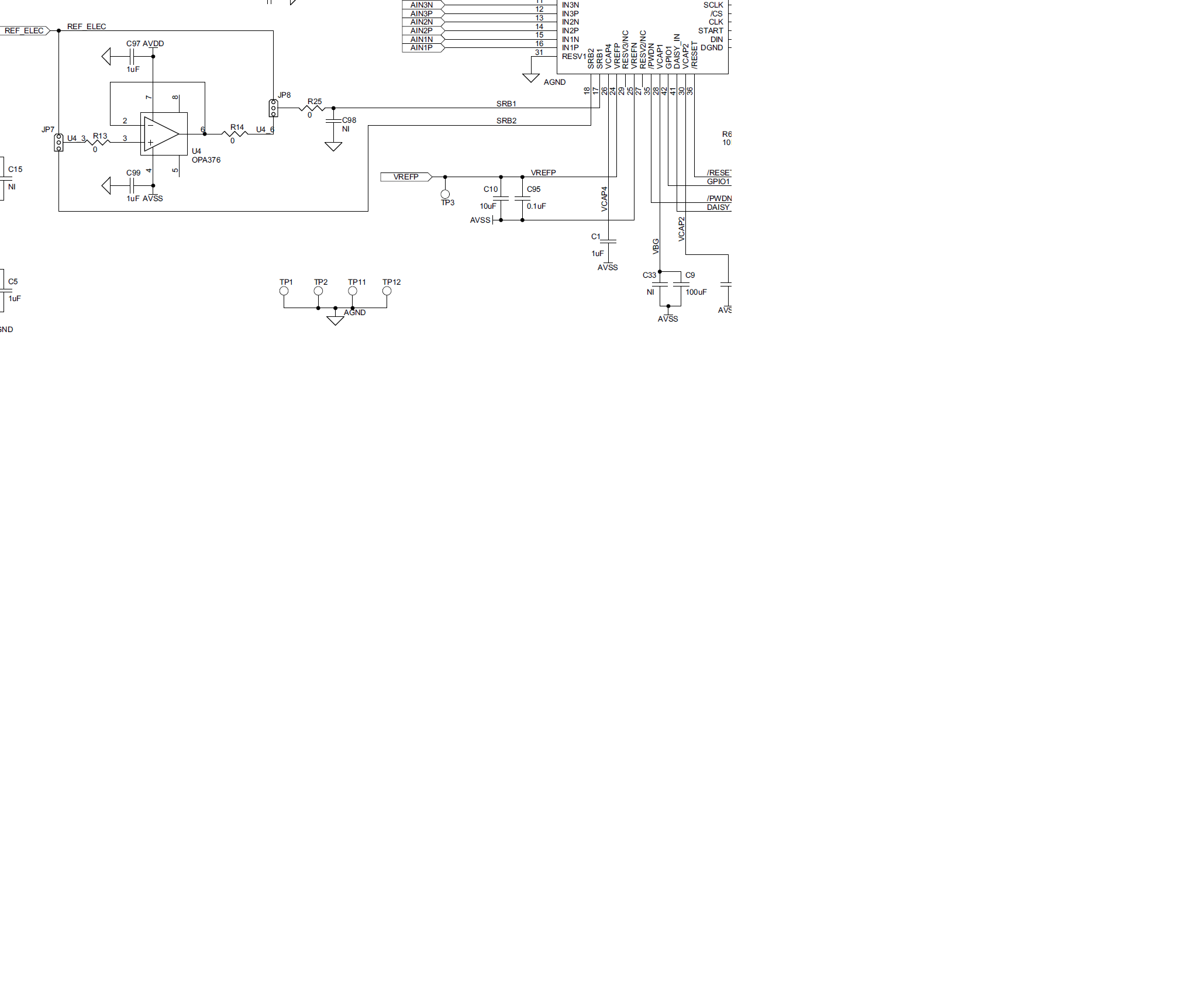
我尝试在 参考电压中找到最佳的输入拓扑,但 我在 TI 文档中找到了两种拓扑
因此、我想知道哪一个更好、还是将这两个相结合?
首先、在 ADS1299数据表中、图73
其次是 ADS1299EEG-FE、图58
您好 Harvey、
感谢您发帖。
我建议遵循图73中所示的示例。 我们最近对这些数据表进行了更新、但它们尚未反映在 EVM 中。 由于 PGA 输入为高阻抗(包括通过 SRBx 的路径)、我不认为需要额外的基准电极缓冲器。 它可能只会增加噪声并使共模抑制性能变差。
此致、


 其次是 ADS1299EEG-FE、图58