This thread has been locked.
If you have a related question, please click the "Ask a related question" button in the top right corner. The newly created question will be automatically linked to this question.
https://e2e.ti.com/support/data-converters-group/data-converters/f/data-converters-forum/1213282/ads8586s-spi-interface-and-ref-schematic
专家、您好!
您能给我们提供 SPI 接口的原理图或应用手册吗?
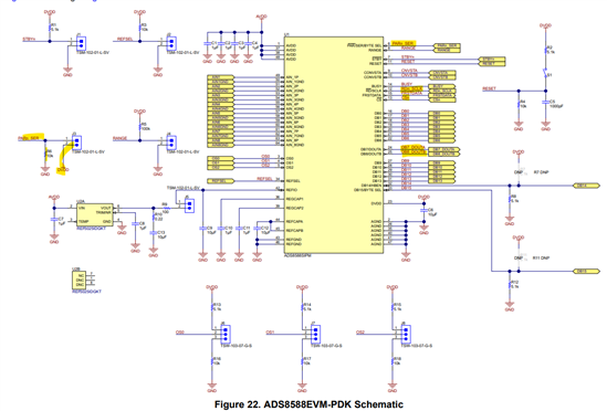
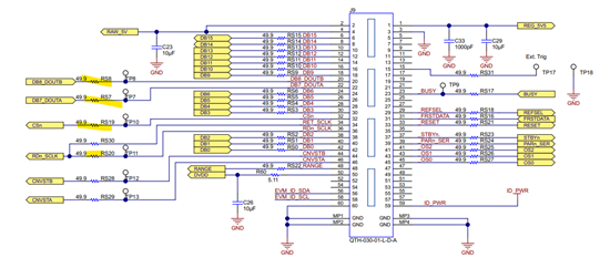
此外、我们需要参考 原理图.
如果否、我们是否必须参考 ADS8588SEVM 用户指南?
此致、
迈克尔
Michael、您好!
此外、我们需要参考 原理图. 如果否、我们是否必须参考 ADS8588SEVM 用户指南? [/报价] 我绝对会使用用户指南作为参考: https://www.ti.com/lit/pdf/sbau278 确认 PAR/SER/BYTE SEL 引脚上的无源上拉或下拉。 您将注意到、除了一个~50ohm 串联电阻外、这些引脚上没有太多可用于平滑快速时钟边沿。 任何器件都不是漏极开路、因此不需要上拉。 如果您有多个器件、并认为您希望 CS 上的上拉电阻是安全的、或者只需依靠在 MCU 上正确设置 GPIO 设置即可。 此致! -Cole.
我绝对会使用用户指南作为参考: https://www.ti.com/lit/pdf/sbau278
确认 PAR/SER/BYTE SEL 引脚上的无源上拉或下拉。
您将注意到、除了一个~50ohm 串联电阻外、这些引脚上没有太多可用于平滑快速时钟边沿。 任何器件都不是漏极开路、因此不需要上拉。 如果您有多个器件、并认为您希望 CS 上的上拉电阻是安全的、或者只需依靠在 MCU 上正确设置 GPIO 设置即可。
此致!
-Cole.