请注意,本文内容源自机器翻译,可能存在语法或其它翻译错误,仅供参考。如需获取准确内容,请参阅链接中的英语原文或自行翻译。
器件型号:ADS131M03 您好!
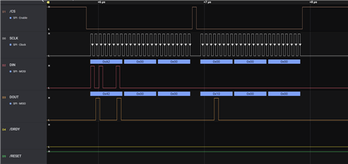
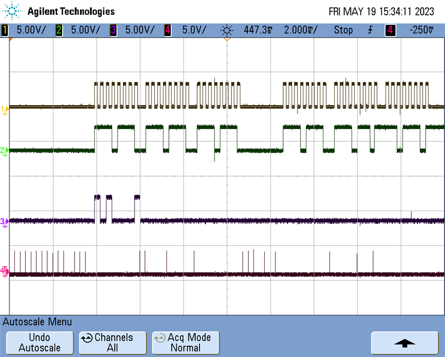
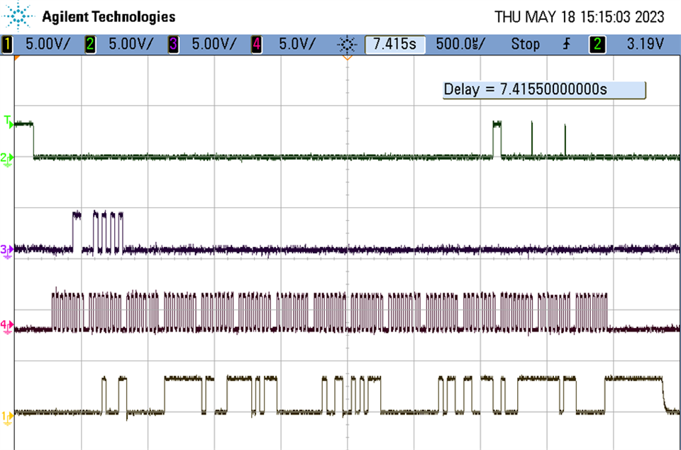
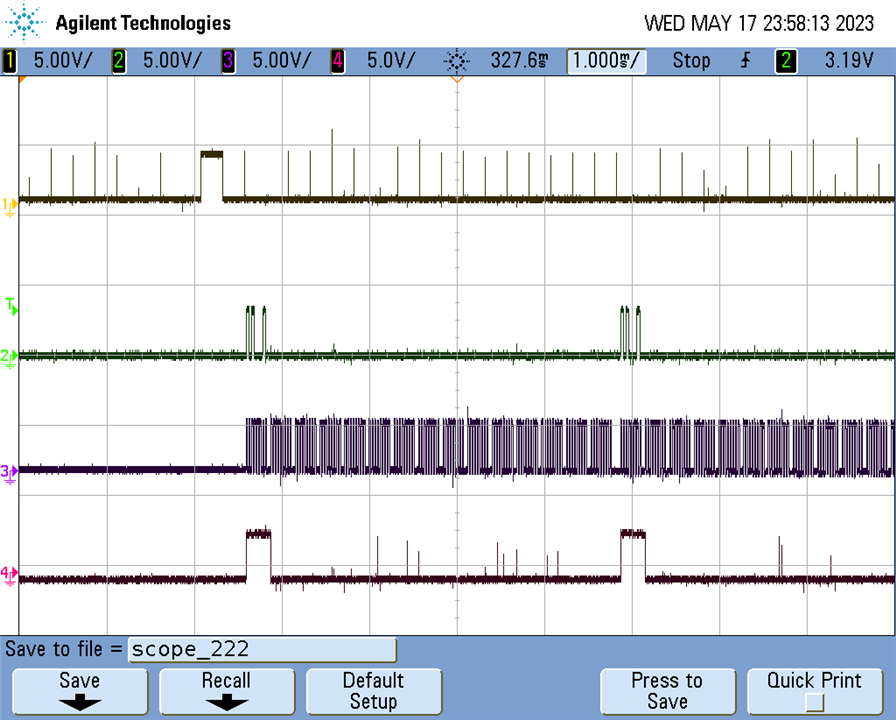
我正在将 ADS131M03 与 Raspberry PI 3B 搭配使用、并通过 Python 编程。 此 ADC 由一个8.192MHz 外部 MEMS 振荡器计时。 SPI 速率设置为32kSPS (我还尝试了3.2k 和320Hz)。 系统之前 在原型板上工作、但在 PCB 上不工作。 捕获的波形如附文所示(第一个:DRDY、第二个:datain、第三个:SCLK、第四个:数据输出)。 我试图读取增益寄存器、 但它返回255个响应、并且没有任何通道数据(尝试读取0x00寄存器时得到相同的结果)、该数据显然不正确。
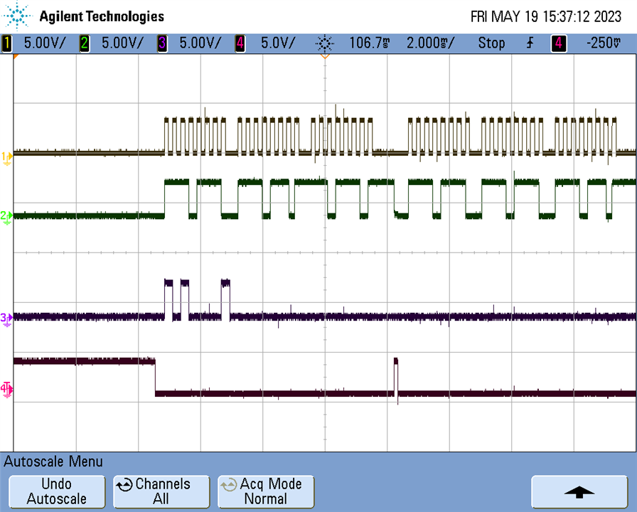
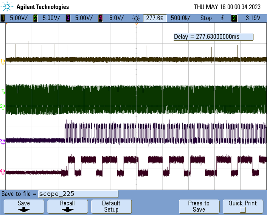
一个有趣的现象是、当我尝试探测到 CLKIN 引脚(连接到外部时钟)时、芯片能够输出读取结果、但每次都不同、捕获的波形被附加:(第一:DRDY、第二:CLKIN、第三:SCLK 4th:Dataout)
已附加我正在使用的代码、我在 RESET 引脚中使用0.0000125延迟来同步、但似乎不起作用。
import time
import spidev
import RPi.GPIO as GPIO
import sys
# clk is a mini class to generate a Master-Clock signal over a PWM Pin


#and also a function which gets two hex numbers and gives back the "Message" for send
#settings
GPIO.setmode(GPIO.BCM)
GPIO.setup(17, GPIO.IN, pull_up_down=GPIO.PUD_UP)   #Pin 17 --> DRDY Pin
GPIO.add_event_detect(17,GPIO.FALLING)

GPIO.setup(8, GPIO.OUT)                             #Pin 8 --> CS'
GPIO.output(8,1)
GPIO.setup(2, GPIO.OUT)                             #Pin 2 --> RESET/SYNC
GPIO.output(2,1)
spi = spidev.SpiDev()

spi.open(0,0)
spi.mode=0b01                                       #CPOL=0, CPHA=1; resting state = 0, data read at falling edge

spi.max_speed_hz =32000
spi.bits_per_word = 8
spi.lsbfirst = False


def read():
    GPIO.output(8,0)
##    time.sleep(0.000125)
##    GPIO.output(2,0)
##    time.sleep(0.000125)
##    GPIO.output(2,1)
##    time.sleep(0.000125)
    send_data = [0b10100000,0b10000000,0b00000000,0b00000000,0b00000000,0b00000000,0b00000000,0b00000000,0b00000000,0b00000000,0b00000000,0b00000000,0b00000000,0b00000000,0b00000000]
    com_reg=spi.xfer2(send_data)


    if GPIO.event_detected(17):
        send_data = [0b10100000,0b10000000,0b00000000,0b00000000,0b00000000,0b00000000,0b00000000,0b00000000,0b00000000,0b00000000,0b00000000,0b00000000,0b00000000,0b00000000,0b00000000]

    # read null response
        com_reg=spi.xfer2(send_data)
##        com_reg=spi.readbytes(15)
        result1 = (8388608-abs(com_reg[3]*256*256+com_reg[4]*256+com_reg[5]-8388608))*0.00000014
        result2 = (8388608-abs(com_reg[6]*256*256+com_reg[7]*256+com_reg[8]-8388608))*0.00000014
        result3 = (8388608-abs(com_reg[9]*256*256+com_reg[10]*256+com_reg[11]-8388608))*0.00000014
        result1 = str(result1)
        result2 = str(result2)
        result3 = str(result3)
        time1 = time.strftime("%H:%M:%S ")
        print("channel1: "+result1+" V")
        print("channel2: "+result2+" V")
        print("channel3: "+result3+" V")
        print("read2")
        print (com_reg)
        file.write("prototest  ")

        file.write(time1)
        file.write("channel1: "+result1+" V  ")

        file.write("channel2: "+result2+" V  ")

        file.write("channel3: "+result3+" V")
        file.write("\n")


    GPIO.output(8, 1)
    time.sleep(1)

def Gain_config():
    GPIO.output(8,0)
    if GPIO.event_detected(17):
        datawreg = [0b01100010, 0b00000000,0b00000000,0b00000000, 0b00000000,0b00000000,0x00,0x00,0x00,0x00,0x00,0x00,0x00,0x00,0x00]
        com_reg=spi.xfer2(datawreg)
        result1 = (8388608-abs(com_reg[3]*256*256+com_reg[4]*256+com_reg[5]-8388608))*0.00000014
        result2 = (8388608-abs(com_reg[6]*256*256+com_reg[7]*256+com_reg[8]-8388608))*0.00000014
        result3 = (8388608-abs(com_reg[9]*256*256+com_reg[10]*256+com_reg[11]-8388608))*0.00000014
        result1 = str(result1)
        result2 = str(result2)
        result3 = str(result3)
        print("channel1: "+result1+" V")
        print("channel2: "+result2+" V")
        print("channel3: "+result3+" V")
        print("gain")
        print (com_reg)

    GPIO.output(8, 1)
    time.sleep(1)
def send_unlock():
# GPIO.output(18, False)
    GPIO.output(8,0)
    if GPIO.event_detected(17):
        send_data = [0b00000110, 0b01010101,0b00000000,0x00,0x00,0x00,0x00,0x00,0x00,0x00,0x00,0x00,0x00,0x00,0x00]
        com_reg=spi.xfer2(send_data)
        print("unlock")
        print (com_reg)
    GPIO.output(8, 1)
    time.sleep(1)
def send_null():
    GPIO.output(8,0)
##    time.sleep(0.000125)
##    GPIO.output(2,0)
##    time.sleep(0.000125)
##    GPIO.output(2,1)
##    time.sleep(0.000125)
    # read null response
##    print("null1")
##    print (com_reg)
    if GPIO.event_detected(17):
        send_data = [0b00000000,0b00000000, 0b00000000,0x00,0x00,0x00,0x00,0x00,0x00,0x00,0x00,0x00,0x00,0x00,0x00]
    # read null response
        com_reg=spi.xfer2(send_data)

##    com_reg=spi.readb
        print("null")
        print (com_reg)
        print (com_reg[12])
        result1 = (8388608-abs(com_reg[3]*256*256+com_reg[4]*256+com_reg[5]-8388608))*0.00000014
        result2 = (8388608-abs(com_reg[6]*256*256+com_reg[7]*256+com_reg[8]-8388608))*0.00000014
        result3 = (8388608-abs(com_reg[9]*256*256+com_reg[10]*256+com_reg[11]-8388608))*0.00000014
        result1 = str(result1)
        result2 = str(result2)
        result3 = str(result3)
        print("channel1: "+result1+" V")
        print("channel2: "+result2+" V")
        print("channel3: "+result3+" V")
    GPIO.output(8, 1)
    time.sleep(1)
def send_reset():
# GPIO.output(18, False)
    GPIO.output(8,0)
##    time.sleep(0.000125)
##    GPIO.output(2,0)
##    time.sleep(0.000125)
##    GPIO.output(2,1)
##    time.sleep(0.000125)
    if GPIO.event_detected(17):
        send_data = [0b00000000, 0b00010001,0b00000000,0x00,0x00,0x00,0x00,0x00,0x00,0x00,0x00,0x00,0x00,0x00,0x00]
        com_reg=spi.xfer2(send_data)
        print("reset2")
        print (com_reg)
    GPIO.output(8, 1)
    time.sleep(1)
def send_wakeup():
# GPIO.output(18, False)
    GPIO.output(8,0)
    if GPIO.event_detected(17):
        send_data = [0b00000000, 0b00110011,0b00000000]
        com_reg=spi.xfer2(send_data)
        print (com_reg)

    GPIO.output(8, 1)
    time.sleep(1)
def Clock_config():
    GPIO.output(8,0)
    if GPIO.event_detected(17):
        datawreg = [0x61,0x80,0x00,0x07,0x0E,0x00,0x00,0x00,0x00,0x00,0x00,0x00,0x00,0x00,0x00]
        dataw=spi.xfer2(datawreg)

        print("clock")
        print (dataw)

    GPIO.output(8, 1)
    time.sleep(1)

def CFG_config():
    GPIO.output(8,0)
    if GPIO.event_detected(17):

    #data write into the CFG Register (Address: 06h)
    #Value written: 0700h, enables Global Chop and sets Global Chop Delay
    #CRC word added, Value = 1021h
    #datawreg = [0x66,0x00,0x07,0x00,0x00,0x00,0x00,0x00,0x00,0x00,0x00,0x00,0x00,0x00,0x00]
        datawreg = [0b01100011, 0b00000000, 0b00000000, 0x07,0x00,0x00,0x10,0x21,0x00,0x00,0x00,0x00,0x00,0x00,0x00]
        dataw=spi.xfer2(datawreg)
        print("cfg")
        print (dataw)

    GPIO.output(8, 1)
    time.sleep(1)

def MODE_config():
    GPIO.output(8,0)
    if GPIO.event_detected(17):
    #data write into the MODE Register (Address: 03h)
    #Value written: 3510h, enables CRC and sets CRC type
    #CRC word added, Value = 1021h
        datawreg = [0b01100001, 0b0000000,0b00000000,0x35,0x10,0x00,0x10,0x21,0x00,0x00,0x00,0x00,0x00,0x00,0x00]
        dataw=spi.xfer2(datawreg)
        print("mode")
        print (dataw)

    GPIO.output(8, 1)
    time.sleep(1)

##
##GPIO.output(8,0)
if GPIO.event_detected(17):
    GPIO.output(2,0)
    time.sleep(0.0000125)
    GPIO.output(2,1)
##read2()
##time.sleep(0.0125)
##GPIO.output(2,0)
##time.sleep(0.000125)
##GPIO.output(2,1)
##########
file = open('/home/pi/Documents/EMILIE/proto517.txt', 'a+')
##send_unlock()
##send_reset()
####
##send_reset()
##Clock_config()
##Gain_config()
########
####send_wakeup()
send_null()
##MODE_config()
##CFG_config()
##
####send_null()
##Gain_config()
while True:
##    GPIO.output(8,0)
    if GPIO.event_detected(17):
        read()
##        send_reset()
##        send_null()
##        send_wakeup()
##
##send_reset()
##Clock_config()
##Gain_config()
##CFG_config()
##send_wakeup()
##send_null()
##MODE_config()
##GPIO.output(8,0)
##while True:
##    if GPIO.event_detected(17):         # Read conversion data
##
##
##
##        data=spi.xfer2([0x00, 0x00, 0x00, 0x00,0x00,0x00,0x00,0x00,0x00,0x00,0x00,0x00,0x00,0x00,0x00])
##        print("receive some Data")
##
##        print(data)


spi.close()
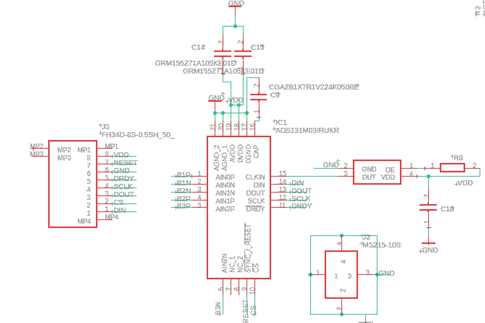
原理图附在后: 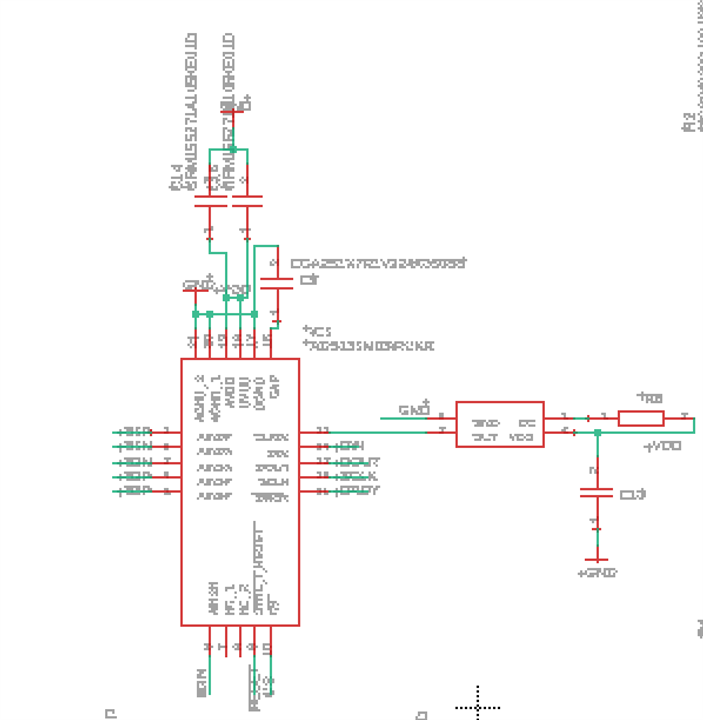
期待收到您的建议!
此致、
Zeyu