This thread has been locked.

If you have a related question, please click the "Ask a related question" button in the top right corner. The newly created question will be automatically linked to this question.

[参考译文] DS90C365A:去耦电容器电容和布局

Guru**** 2477065 points


请注意,本文内容源自机器翻译,可能存在语法或其它翻译错误,仅供参考。如需获取准确内容,请参阅链接中的英语原文或自行翻译。

https://e2e.ti.com/support/interface-group/interface/f/interface-forum/1555497/ds90c365a-decoupling-capacitor-capacitance-and-layout

器件型号:DS90C365A


工具/软件:

请告诉我是否有任何规格、例如去耦电容器的数量、电容值、布局布线等

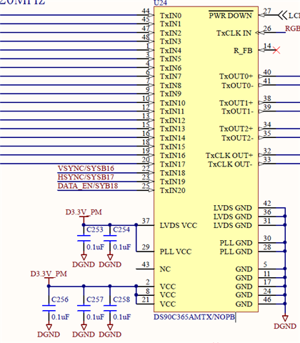
目前、当前设计是在每个电源引脚(37 引脚、29 引脚、2 引脚、8 引脚、21 引脚)上安装一个 0.1uF(0603 仪表)。

输入侧为 RGB666(21 位)、计划在 20MHz 上使用。

  • 请注意,本文内容源自机器翻译,可能存在语法或其它翻译错误,仅供参考。如需获取准确内容,请参阅链接中的英语原文或自行翻译。

    您好:

    我们建议使用与 Flink EVM 类似的去耦网络: https://www.ti.com/lit/ug/snlu032a/snlu032a.pdf

    Vcc 引脚应具有多个电容器、包括连接到每个引脚的较大电容器(22uF 电容器)。
    20MHz 像素时钟速率在支持 18 至 87.5MHz 的器件规格范围内。

    此致、
    Ikram