
Other Parts Discussed in Thread: SN75LVDS83B, SN75LVDS83
主题中讨论的其他器件: SN75LVDS83
大家好、
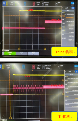
客户测试 SN75LVDS83B 及其 LVDS CLKOUT、客户发现在没有 RGB 输入的情况下应用 VDD 时、CLKOUT 的状态是什么? 客户测试结果如下、您能否帮助解释 CLKOUT 为何摆动在共模电压附近? 顶部是竞争对手测试结果、底部是 TI 结果。
Thx~
Rayna
This thread has been locked.
If you have a related question, please click the "Ask a related question" button in the top right corner. The newly created question will be automatically linked to this question.
Other Parts Discussed in Thread: SN75LVDS83B, SN75LVDS83
大家好、
客户测试 SN75LVDS83B 及其 LVDS CLKOUT、客户发现在没有 RGB 输入的情况下应用 VDD 时、CLKOUT 的状态是什么? 客户测试结果如下、您能否帮助解释 CLKOUT 为何摆动在共模电压附近? 顶部是竞争对手测试结果、底部是 TI 结果。


Thx~
Rayna
您好、Rayna、
[报价 userid="417933" URL"~/support/interface-group/interface/f/interface-forum/1160035/sn75lvds83b-what-s-the-status-of-clock-output-when-vdd-is-applied/4364839 #4364839"]您是否怀疑这会受到其他设备的影响?CLKOUT 摆幅是否会对下游器件(DES、DISPLAY)造成任何影响?
[引用 userid="417933" URL"~/support/interface-group/interface/f/interface-forum/1160035/sn75lvds83b-what-s-the-status-of-clock-output-when-vdd-is-applied/4364839 #4364839">其 LVDSCLK 输出的状态是什么? 它是内部上拉还是下拉、还是三态?[/quot]众所周知、当 SHTDN 为低电平时、LVDSCLK 输出为高阻抗。 鉴于此器件的使用寿命、我无法在数据表中找到更多信息。
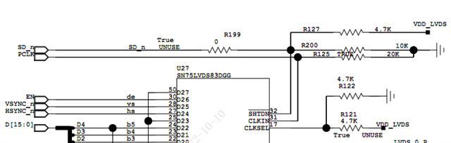
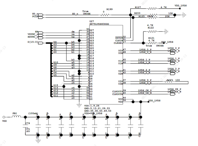
您能否附加 SN75LVDS83B 的原理图?
此致、
插孔