This thread has been locked.
If you have a related question, please click the "Ask a related question" button in the top right corner. The newly created question will be automatically linked to this question.
Other Parts Discussed in Thread: UCC5320
https://e2e.ti.com/support/interface-group/interface/f/interface-forum/672055/ucc5320-pcb-layout-example
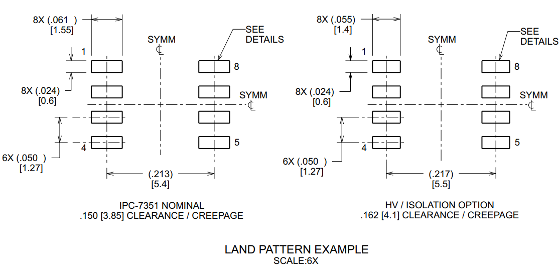
大家好、在 UCC5320数据表第46页中、我们有下图。
左侧和右侧之间的区别是什么? 绘制 PCB 时、应遵循哪一侧?
您好 Howard、 左侧和右侧之间的差异是焊盘的长度。 这会影响数据表第7页隔离表上的爬电距离和间隙。
使用右侧[4.1]爬电距离和间隙来满足 HV 布局和隔离需求。 对于低电压、可接受较小的爬电距离和间隙[3.85]。 如果您的问题得到了解答、请按绿色按钮。 此致、 Mateo


