

Other Parts Discussed in Thread: SN6507
请注意,本文内容源自机器翻译,可能存在语法或其它翻译错误,仅供参考。如需获取准确内容,请参阅链接中的英语原文或自行翻译。
https://e2e.ti.com/support/isolation-group/isolation/f/isolation-forum/1161202/sn6507-pcb-layout
器件型号:SN6507您好!
以下 PCB 布局是否正常?
SW1位于底部、SW2位于顶部。
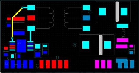
谢谢。
Other Parts Discussed in Thread: SN6507
https://e2e.ti.com/support/isolation-group/isolation/f/isolation-forum/1161202/sn6507-pcb-layout
器件型号:SN6507您好!
以下 PCB 布局是否正常?
SW1位于底部、SW2位于顶部。
谢谢。
