
This thread has been locked.

If you have a related question, please click the "Ask a related question" button in the top right corner. The newly created question will be automatically linked to this question.

[参考译文] DRV2700:反激式模式 — CAN 't 达到 0V

Guru**** 2939240 points

Other Parts Discussed in Thread: DRV2700

请注意,本文内容源自机器翻译,可能存在语法或其它翻译错误,仅供参考。如需获取准确内容,请参阅链接中的英语原文或自行翻译。

https://e2e.ti.com/support/motor-drivers-group/motor-drivers/f/motor-drivers-forum/1652616/drv2700-flyback-mode---can-t-reach-0v

部件号: DRV2700

尊敬的团队:

我们希望为我们的工程设计一个 0V 至 200V 的正弦波输出、因此我们选择了反激模式的 DRV2700。

我们在 TINA 软件中设计和仿真了电路。 我们将达到 200V、但输出不是纯正弦波、也不会达到 0V、而是从大约 50V 摆动。 我们需要精确的 0V 到 200V 正弦波输出。

我随附了波形和设计图像以供参考。
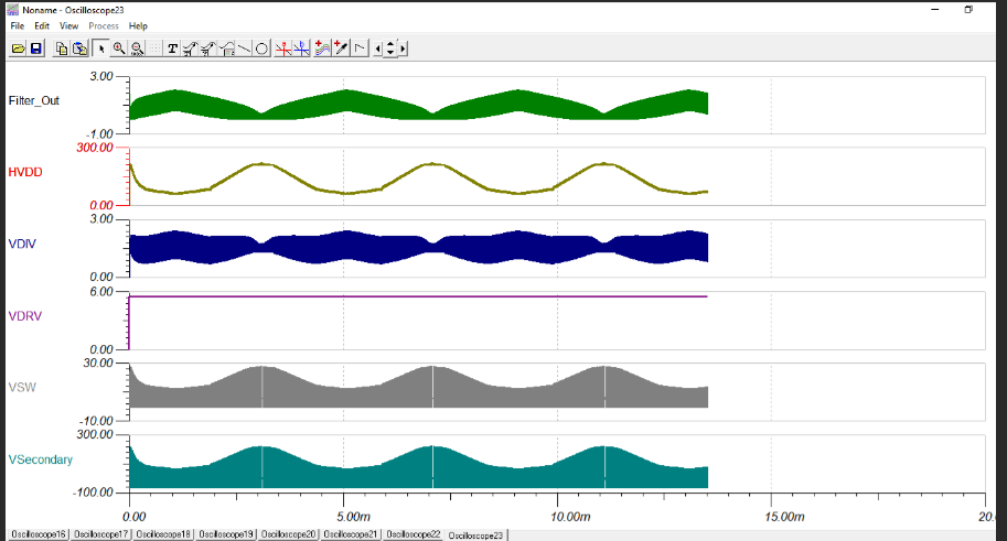
image.png

  • 请注意,本文内容源自机器翻译,可能存在语法或其它翻译错误,仅供参考。如需获取准确内容,请参阅链接中的英语原文或自行翻译。

    Kannan、  

    感谢您的联系。 您能分享这个设计图像吗? 我只看到了波形图像。  

  • 请注意,本文内容源自机器翻译,可能存在语法或其它翻译错误,仅供参考。如需获取准确内容,请参阅链接中的英语原文或自行翻译。

    尊敬的团队:

    FYR、


  • 请注意,本文内容源自机器翻译,可能存在语法或其它翻译错误,仅供参考。如需获取准确内容,请参阅链接中的英语原文或自行翻译。


    尊敬的团队:
    供参考

  • 请注意,本文内容源自机器翻译,可能存在语法或其它翻译错误,仅供参考。如需获取准确内容,请参阅链接中的英语原文或自行翻译。

    ",="" roboto,="" arial,="" sans-serif;="" font-size:="" 16px;="" font-weight:="" 400;="" margin:="" 0px;="" text-decoration:="" none;="" border-bottom:="" 0px="" rgb(10,="" 10,="" 10);"=""> ",="" roboto,="" arial,="" sans-serif;="" font-size:="" 16px;="" font-weight:="" 400;="" margin:="" 0px;="" text-decoration:="" none;="" border-bottom:="" 0px="" rgb(10,="" 10,="" 10);"="">DRV2700 利用迟滞式开关稳压器。 即使模拟控制信号指定 0V 电压、器件也会保持最小开关脉冲宽度、以使其内部环路保持有效。  这种持续开关会持续将基线能量泵入反激式变压器次级绕组。 结合漏电感和输出二极管电容、残余直流电荷会在高压输出电容器 C4 上积累。  由于电路没有用于对 C4 进行放电的有源下拉机制、因此该残余能量会导致输出电压稳定在最小本底电压(通常约为 40V 至 50V)。  

    要完全解决 TINA 软件设计中的问题、请进行以下电路修改

    ",="" roboto,="" arial,="" sans-serif;="" font-size:="" 16px;="" font-weight:="" 600;="" margin:="" 24px="" 0px="" 12px;="" text-decoration:="" none;="" border-bottom:="" rgb(10,="" 10,="" 10);"="">选项 A:使用差分(桥接负载)驱动器配置:

    您应该使用 H 桥输出级差分驱动压电式、而不是单端驱动圆盘泵(一侧连接到 GND)。  

      ",="" roboto,="" arial,="" sans-serif;="" font-size:="" 16px;="" font-weight:="" 400;="" margin:="" 12px="" 0px="" text-decoration:="" none;="" border-bottom:="" rgb(10,="" 10,="" 10);"="">
    • ",="" roboto,="" arial,="" sans-serif;="" font-size:="" 16px;="" font-weight:="" 400;="" margin:="" 0px="" 12px;="" text-decoration:="" none;="" border-bottom:="" rgb(10,="" 10,="" 10);"="">",="" roboto,="" arial,="" sans-serif;="" font-size:="" 16px;="" font-weight:="" 400;="" margin:="" 0px;="" text-decoration:="" none;="" border-bottom:="" 0px="" rgb(10,="" 10,="" 10);"="">通过使用两个异相高压电源轨或利用次级高压半桥、您可以将负载上的电压拉低至 0V 净差分 摆幅。 此技术可以消除两个端子上的基线直流失调电压。
    ",="" roboto,="" arial,="" sans-serif;="" font-size:="" 16px;="" font-weight:="" 600;="" margin:="" 24px="" 0px="" 12px;="" text-decoration:="" none;="" border-bottom:="" rgb(10,="" 10,="" 10);"="">选项 B:添加主动泄放/恒定电流阱
    ",="" roboto,="" arial,="" sans-serif;="" font-size:="" 16px;="" font-weight:="" 400;="" margin:="" 12px="" 0px="" text-decoration:="" none;="" border-bottom:="" rgb(10,="" 10,="" 10);"="">如果必须保持单端输出架构、则需要添加一个小型有源电流阱来抵消最小脉冲宽度能量插入。
      ",="" roboto,="" arial,="" sans-serif;="" font-size:="" 16px;="" font-weight:="" 400;="" margin:="" 12px="" 0px="" text-decoration:="" none;="" border-bottom:="" rgb(10,="" 10,="" 10);"="">
    • ",="" roboto,="" arial,="" sans-serif;="" font-size:="" 16px;="" font-weight:="" 400;="" margin:="" 0px="" 12px;="" text-decoration:="" none;="" border-bottom:="" rgb(10,="" 10,="" 10);"="">",="" roboto,="" arial,="" sans-serif;="" font-size:="" 16px;="" font-weight:="" 400;="" margin:="" 0px;="" text-decoration:="" none;="" border-bottom:="" 0px="" rgb(10,="" 10,="" 10);"="">修改: 将配置为恒流阱 的高压晶体管(例如耗尽型 MOSFET 或高压 BJT)与输出电容器 C4 并联。
    • ",="" roboto,="" arial,="" sans-serif;="" font-size:="" 16px;="" font-weight:="" 400;="" margin:="" 0px="" 12px;="" text-decoration:="" none;="" border-bottom:="" rgb(10,="" 10,="" 10);"="">",="" roboto,="" arial,="" sans-serif;="" font-size:="" 16px;="" font-weight:="" 400;="" margin:="" 0px;="" text-decoration:="" none;="" border-bottom:="" 0px="" rgb(10,="" 10,="" 10);"="">结果: 该有源负载 在正弦波周期的最下部安全地将输出节点下拉至真正的 0V 状态、从而消除 50V 基线偏移。
    ",="" roboto,="" arial,="" sans-serif;="" font-size:="" 14px;="" font-weight:="" 400;="" margin:="" 0px;="" text-decoration:="" none;="" border-bottom:="" 0px="" rgb(10,="" 10,="" 10);"="">