请注意,本文内容源自机器翻译,可能存在语法或其它翻译错误,仅供参考。如需获取准确内容,请参阅链接中的英语原文或自行翻译。
器件型号:MSP430F5132 各位专家、您好!
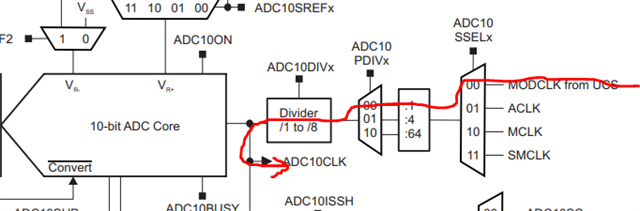
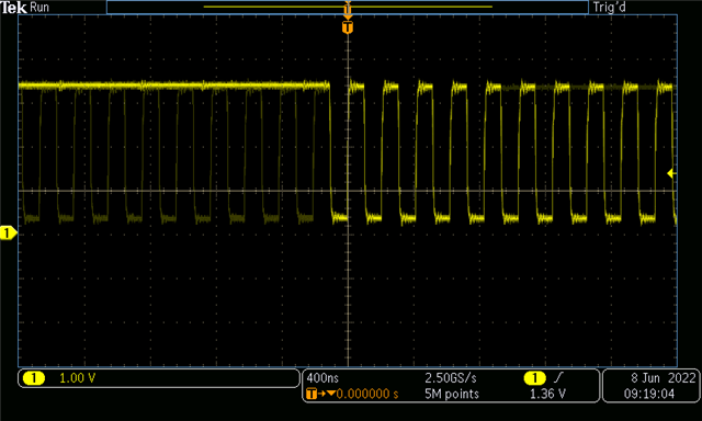
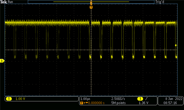
我正在探测 PJ.2以查看 ADC10CLK、波形不是预期的。 有什么想法为什么这么做?
1) 1)我不使用调试器。 (使用调试器之前 使8MHz MCLK 看起来很奇怪)
2) 2)在探测 J.0时、MCLK 看起来非常完美
3) 3) SMCLK 在探测 J.1时与 ADC10CLK 具有相同的奇数行为
4) 4)在缩小的范围捕获上看到抖动。
ADC10CLK (PJ.2)示波器捕捉已缩小:
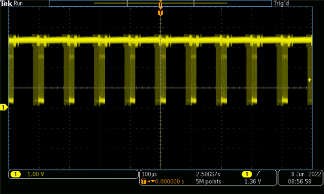
放大的 ADC10CLK (PJ.2)示波器捕捉。 左半部分闪烁开/关:
随附相关代码:
//                                   MSP430F51x2
//                                -----------------
//                            /|\|                 |
//                             | |                 |
//                             --|RST              |
//     GPIO to trip relay <-- (1)|P1.0        PJ.0 | (7) --> SMCLK (debug)
//               AC + DC  >---(2)|P1.1/A1     PJ.1 | (8) --> MCLK  (debug)
//   GPIO to debug TimerA <-- (4)|P1.3        PJ.2 | (9) --> ADC10CLK (debug)

    PJSEL |= BIT0 + BIT1 + BIT2;    //Output CLKs to PJ.0-2
    PJDIR |= BIT0 + BIT1 + BIT2;

    // configure clocks
    UCSCTL3 = SELREF_2;                       // Set DCO FLL reference = REFO
    UCSCTL4 |= SELA_2;                        // Set ACLK = REFO

    __bis_SR_register(SCG0);                  // Disable the FLL control loop
    UCSCTL0 = 0x0000;                         // Set lowest possible DCOx, MODx
    UCSCTL1 = DCORSEL_5;                      // Select DCO range 16MHz operation
    UCSCTL2 = FLLD_1 + 243;                   // Set DCO Multiplier for 8MHz
                                            // (N + 1) * FLLRef = Fdco
                                            // (243 + 1) * 32768 = 8MHz
    __bic_SR_register(SCG0);                 // re-enable the FLL control loop

    // Worst-case settling time for the DCO when the DCO range bits have been
    // changed is n x 32 x 32 x f_MCLK / f_FLL_reference. See UCS chapter in 5xx
    // UG for optimization.
    // 32 x 32 x 8 MHz / 32,768 Hz = 250000 = MCLK cycles for DCO to settle
    __delay_cycles(250000);

    // Loop until XT1 & DCO stabilizes - In this case only DCO has to stabilize
    do
    {
    UCSCTL7 &= ~(XT1LFOFFG + XT1HFOFFG + DCOFFG);
                                            // Clear XT1,DCO fault flags
    SFRIFG1 &= ~OFIFG;                      // Clear fault flags
    }while (SFRIFG1&OFIFG);                   // Test oscillator fault flag


    P1DIR |= BIT0 +BIT3;                    // Set P1.0, P1.3 output direction
    P1OUT &= ~BIT0;                         // Clear P1.0

    // Configure internal reference
    while(REFCTL0 & REFGENBUSY);            // If ref generator busy, WAIT
    REFCTL0 |= REFVSEL_0+REFON;             // Select internal ref = 1.5V
                                            // Set FSR of ADC10 for ADC10SREF

    __delay_cycles(100);                     // Delay for Ref to settle

    // Configure ADC10
    ADC10CTL0 &= ~ADC10ENC;                 // Disable ADC
    ADC10CTL0 |= ADC10SHT_2;                // clk cycles per sample period
    ADC10CTL0 |= ADC10ON;                   // enable ADC10
    ADC10CTL1 |= ADC10SSEL_0;               // ADC clock = MODCLK = 5MHz
    ADC10CTL1 |= ADC10SHP;                  // pulse sample mode
    ADC10CTL1 |= ADC10CONSEQ_0;             // single-conversion, single-channel mode 27.2.7
    ADC10CTL1 |= ADC10SHS_0;                // triggered sample with ADC10SC
    ADC10CTL2 |= ADC10RES;                  // 10-bit conversion results
    ADC10MCTL0 = 0;
    ADC10MCTL0 |= ADC10SREF_1;              // (REF_x) V+ = Vref+, V- = AVSS
    ADC10MCTL0 |= ADC10INCH_1;              // Read ch 1 (P1.1)
    ADC10IE |= ADC10IFG0;                   // Interrupt enable
    ADC10CTL0 |= ADC10ENC + ADC10SC;        // Enable ADC and trigger ADC read