Other Parts Discussed in Thread: MSP430FR2433
请注意,本文内容源自机器翻译,可能存在语法或其它翻译错误,仅供参考。如需获取准确内容,请参阅链接中的英语原文或自行翻译。
器件型号:MSP430FR2433 我正在尝试使用 TIMER_A_ex1_pwmSingle 示例作为模板将 P1.1设置为 PWM 输出。
我一直在讨论如何将 P1.1初始化为 PWM 输出。
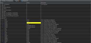
根据我的理解、我需要设置寄存器 P1DIR = 0b01和寄存器 P1SEL1 = 0b01、以将 P1.1初始化为 PWM 输出。
函数时的示例
GPIO_setPeripheralModuleFunctionOutputPin (
GPIO_PORT_P1、
GPIO_PIN1、
GPIO_secondary 模块功能
);
而是以 P1SEL0寄存器为目标。
如前面提到的示例中所示、将 P1.1配置为 PWM 输出需要做什么?
下面是我的代码-首先让我们重点介绍71 - 76行、我尝试将 P1.1初始化为 PWM 输出。
/* --COPYRIGHT--,BSD
* Copyright (c) 2017, Texas Instruments Incorporated
* All rights reserved.
*
* Redistribution and use in source and binary forms, with or without
* modification, are permitted provided that the following conditions
* are met:
*
* * Redistributions of source code must retain the above copyright
* notice, this list of conditions and the following disclaimer.
*
* * Redistributions in binary form must reproduce the above copyright
* notice, this list of conditions and the following disclaimer in the
* documentation and/or other materials provided with the distribution.
*
* * Neither the name of Texas Instruments Incorporated nor the names of
* its contributors may be used to endorse or promote products derived
* from this software without specific prior written permission.
*
* THIS SOFTWARE IS PROVIDED BY THE COPYRIGHT HOLDERS AND CONTRIBUTORS "AS IS"
* AND ANY EXPRESS OR IMPLIED WARRANTIES, INCLUDING, BUT NOT LIMITED TO,
* THE IMPLIED WARRANTIES OF MERCHANTABILITY AND FITNESS FOR A PARTICULAR
* PURPOSE ARE DISCLAIMED. IN NO EVENT SHALL THE COPYRIGHT OWNER OR
* CONTRIBUTORS BE LIABLE FOR ANY DIRECT, INDIRECT, INCIDENTAL, SPECIAL,
* EXEMPLARY, OR CONSEQUENTIAL DAMAGES (INCLUDING, BUT NOT LIMITED TO,
* PROCUREMENT OF SUBSTITUTE GOODS OR SERVICES; LOSS OF USE, DATA, OR PROFITS;
* OR BUSINESS INTERRUPTION) HOWEVER CAUSED AND ON ANY THEORY OF LIABILITY,
* WHETHER IN CONTRACT, STRICT LIABILITY, OR TORT (INCLUDING NEGLIGENCE OR
* OTHERWISE) ARISING IN ANY WAY OUT OF THE USE OF THIS SOFTWARE,
* EVEN IF ADVISED OF THE POSSIBILITY OF SUCH DAMAGE.
* --/COPYRIGHT--*/
//*******************************************************************************
//! Timer_A3, PWM TA1.2, Up Mode, DCO SMCLK
//!
//! Description: This program generates PWM outputs on P2.2 using
//! Timer1_A configured for up mode. The value , TIMER_PERIOD, defines the PWM
//! period and the value DUTY_CYCLE the PWM duty cycle. Using ~1.048MHz
//! SMCLK as TACLK, the timer period is ~480us with a 75% duty cycle on P4.0
//! ACLK = n/a, SMCLK = MCLK = TACLK = default DCO ~1.048MHz.
//!
//! Tested On: MSP430FR4133
//! -------------------
//! /|\| |
//! | | |
//! --|RST |
//! | |
//! | P4.0/TA1.1|--> CCR1 - 75% PWM
//! | |
//!
//! This example uses the following peripherals and I/O signals. You must
//! review these and change as needed for your own board:
//! - Timer peripheral
//! - GPIO peripheral
//!
//! This example uses the following interrupt handlers. To use this example
//! in your own application you must add these interrupt handlers to your
//! vector table.
//! - NONE
//******************************************************************************
#include "driverlib.h"
#define TIMER_A_PERIOD 524
#define DUTY_CYCLE 393
void main (void)
{
//Stop WDT
WDT_A_hold(WDT_A_BASE);
//P1.1 as PWM output
GPIO_setAsPeripheralModuleFunctionOutputPin(
GPIO_PORT_P1,
GPIO_PIN1,
GPIO_SECONDARY_MODULE_FUNCTION
);
/*
* Disable the GPIO power-on default high-impedance mode to activate
* previously configured port settings
*/
PMM_unlockLPM5();
//Generate PWM - Timer runs in Up-Down mode
Timer_A_outputPWMParam param = {0};
param.clockSource = TIMER_A_CLOCKSOURCE_SMCLK;
param.clockSourceDivider = TIMER_A_CLOCKSOURCE_DIVIDER_1;
param.timerPeriod = TIMER_A_PERIOD;
param.compareRegister = TIMER_A_CAPTURECOMPARE_REGISTER_1;
param.compareOutputMode = TIMER_A_OUTPUTMODE_RESET_SET;
param.dutyCycle = DUTY_CYCLE;
Timer_A_outputPWM(TIMER_A1_BASE, ¶m);
//Enter LPM0
__bis_SR_register(LPM0_bits);
//For debugger
__no_operation();
}