This thread has been locked.

If you have a related question, please click the "Ask a related question" button in the top right corner. The newly created question will be automatically linked to this question.

[参考译文] MSP430FR4133:MSP430FR4133多 ADC 采样行为不符合使用示例的预期

Guru**** 657930 points
Other Parts Discussed in Thread: MSP430FR4133
请注意,本文内容源自机器翻译,可能存在语法或其它翻译错误,仅供参考。如需获取准确内容,请参阅链接中的英语原文或自行翻译。

https://e2e.ti.com/support/microcontrollers/msp-low-power-microcontrollers-group/msp430/f/msp-low-power-microcontroller-forum/1219319/msp430fr4133-msp430fr4133-multiple-adc-sampling-not-behaving-as-expected-using-example

器件型号:MSP430FR4133

大家好、我一直在尝试使用适用于 MSP430FR4133的 ADC 模块实施模拟双轴操纵杆、我已经开始连接两个电位器进行测试。 我已经遵循了 slac625h 库中的示例代码"msp430fr413x_adc10_10.c"示例。 我唯一更改的是从8位转换更改为10位转换、以及 int 格式、ADCSRF_0更改为 AVCC、AVSS。  

代码:   

#include <msp430.h>

unsigned int ADC_Result[3];                                    // 8-bit ADC conversion result array
unsigned int i;

int main(void)
{
    WDTCTL = WDTPW | WDTHOLD;                                   // Stop WDT
    
    // Configure ADC A0~2 pins
    SYSCFG2 |= ADCPCTL0 | ADCPCTL1 | ADCPCTL2;
  
    // Disable the GPIO power-on default high-impedance mode to activate
    // previously configured port settings
    PM5CTL0 &= ~LOCKLPM5;

    // Configure ADC 
    ADCCTL0 |= ADCSHT_2 | ADCON;                                // 16ADCclks, ADC ON
    ADCCTL1 |= ADCSHP | ADCSSEL_1 | ADCSHS_2 | ADCCONSEQ_3;                 // ADC clock MODCLK, sampling timer, TA1.1B trig.,repeat sequence
    ADCCTL2 |= ADCRES;                                         // 10-bit conversion results
    ADCMCTL0 |= ADCINCH_2 | ADCSREF_0;                          // A0~2(EoS); Vref=Vcc
    ADCIE |= ADCIE0;                                            // Enable ADC conv complete interrupt
    
    // Configure reference
    PMMCTL0_H = PMMPW_H;                                        // Unlock the PMM registers
    PMMCTL2 |= INTREFEN;                                        // Enable internal reference
    __delay_cycles(400);                                        // Delay for reference settling
    __no_operation();

    // Configure TA1.1B as ADC trigger signal
    // Note: The TA1.1B is configured for 200us 50% PWM, which will trigger ADC
    // sample-and-conversion every 200us. The period of TA1.1B trigger event
    // should be more than the time period taken for ADC sample-and-conversion
    // and ADC interrupt service routine of each channel, which is about 57us in this code
    TA1CCR0 = 200-1;                                            // PWM Period, 200us
    TA1CCTL1 = OUTMOD_7;                                        // CCR1 reset/set
    TA1CCR1 = 100;                                              // CCR1 PWM duty cycle, 50%
    TA1CTL = TASSEL__SMCLK | MC__UP | TACLR;                    // SMCLK, up mode, clear TAR

    while(1)                                
    {
        i = 2;

        ADCCTL0 |= ADCENC;                                      // Enable ADC
        TA1CTL |= TACLR;                                        // Clear TAR to start the ADC sample-and-conversion
        __bis_SR_register(LPM0_bits | GIE);                     // Enter LPM0 w/ interrupts
        __no_operation();                                       // Only for debugger

    }
}

// ADC interrupt service routine
#if defined(__TI_COMPILER_VERSION__) || defined(__IAR_SYSTEMS_ICC__)
#pragma vector=ADC_VECTOR
__interrupt void ADC_ISR(void)
#elif defined(__GNUC__)
void __attribute__ ((interrupt(ADC_VECTOR))) ADC_ISR (void)
#else
#error Compiler not supported!
#endif
{
    switch(__even_in_range(ADCIV,ADCIV_ADCIFG))
    {
        case ADCIV_NONE: 
            break;                              
        case ADCIV_ADCOVIFG: 
            break;             
        case ADCIV_ADCTOVIFG: 
            break;            
        case ADCIV_ADCHIIFG: 
            break;             
        case ADCIV_ADCLOIFG: 
            break;             
        case ADCIV_ADCINIFG: 
            break;             
        case ADCIV_ADCIFG:
            ADC_Result[i] = ADCMEM0;
            if(i == 0)
            {
                __no_operation();                               // Only for debugger
                i = 2;
            }
            else
            {
                i--;
            }
            break;                                             
        default: 
            break; 
    }  
}

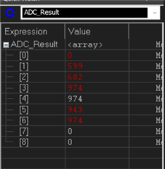
我在过去几天一直在这里,但我似乎不能完全包裹我的头,为什么 A0读数似乎不是从电位器正确的读数。 但 A1读数似乎是完美的。 A2仅为 P1.2按钮(工作正常;按下时显示0)。  

下面是我的接线图:

(为糟糕的图表道歉)

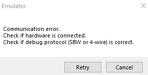
我还注意到另一个异常情况、如果我在 A0上将电位器修整得太远(10k)、IAR 会向我显示以下错误、并且我的程序在调试期间只是挂起:

我尝试使用替代电位计、但错误相同。  

非常感谢您的参与!

亚伦  

  • 请注意,本文内容源自机器翻译,可能存在语法或其它翻译错误,仅供参考。如需获取准确内容,请参阅链接中的英语原文或自行翻译。

    您正在使用什么平台? 如果您使用的是 Launchpad、您是否断开了 LED1与 P1.0的连接?

  • 请注意,本文内容源自机器翻译,可能存在语法或其它翻译错误,仅供参考。如需获取准确内容,请参阅链接中的英语原文或自行翻译。

    您好、感谢您的回复、是的、我正在使用 MSP430FR4133 Launchpad、通过断开 LED1、我假设旁边的跳线连接器(JP1)已经将其移除、仍然可以观察到相同的行为。  

  • 请注意,本文内容源自机器翻译,可能存在语法或其它翻译错误,仅供参考。如需获取准确内容,请参阅链接中的英语原文或自行翻译。

    A0得到了什么结果? 即、您的测试顺序是什么?

    ----------------

    > ADCCTL1 |= ADCSHP | ADCSSEL_1 | ADCSHS_2 | ADCCONSEQ_3;// ADC 时钟 MODCLK、采样计时器、TA1.1B 触发、重复序列

    ADCSSEL=1将 ADC 时钟设置为 ACLK (32kHz)、因此转换需要(16+13)* 30.5us=885us、但触发每200us 关闭一次、因此您将获得触发溢出(ADCTOV)。 用户指南并未真正描述此情况下发生的情况。 我建议您将其改回  

    > ADCCTL1 |= ADCSHP | ADCSSEL_0 | ADCSHS_2 | ADCCONSEQ_3;// ADC 时钟 MODCLK、采样计时器、TA1.1B 触发、重复序列

    [我正在将您的代码与以下代码进行比较:

    https://dev.ti.com/tirex/explore/node?node=A__AE84sEwNMQaWLxkyStgOPg__msp430ware__IOGqZri__LATEST

    ]

  • 请注意,本文内容源自机器翻译,可能存在语法或其它翻译错误,仅供参考。如需获取准确内容,请参阅链接中的英语原文或自行翻译。

    抱歉、我应该已经发布了结果、它们位于此处:  

    A1工作正常(电位器一直修整为0)、A0是有问题的器件、A2是按钮(将光标悬停在该值附近、除非在这种情况下按下会变为0)。  

    将 A1电位器调至最大值后、在发生规定的错误之前将 A0调至最大值、并按下 A2按钮:  

    我也根据您的建议将其改回 MODCLK。 因此、A2和 A1的读数似乎很好。

  • 请注意,本文内容源自机器翻译,可能存在语法或其它翻译错误,仅供参考。如需获取准确内容,请参阅链接中的英语原文或自行翻译。

    我不是 EE、但我建议您不要将 POT 设置为0欧姆、因为这看起来像是一个短路(这可能会导致电路板和调试器发生故障)。 Ax 引脚大部分为高阻抗、但 GND 引脚不是高阻抗。 我想上次我使用电位计时、我从它中间制作了一个电阻分压器、正是出于这个原因。

    更一般地说、电位计的一个危害是、很容易最终选择阻抗相当高的源、这将需要更长的采样/保持时间来为 ADC 电容器充电。 UG (SLAU445I)第21.2.5.3节提供了一个公式、但快速实验将 ADCSHT 设置为非常高、并查看症状是否发生变化。 (这也可能会增加您的计时器触发周期、因此您可能也希望增加该周期。)

    另一个快速实验是设置 ADCINCH=0、以查看 A0在隔离方面是否工作得更好。

  • 请注意,本文内容源自机器翻译,可能存在语法或其它翻译错误,仅供参考。如需获取准确内容,请参阅链接中的英语原文或自行翻译。

    我刚刚注意到、P1.0也通过 J101 ("桥接跳线块")连接到反向通道 UART。 我建议拔下 TXD 和 RXD 跳线;P1.1 (RXD)不受影响、我感到有点惊讶。

  • 请注意,本文内容源自机器翻译,可能存在语法或其它翻译错误,仅供参考。如需获取准确内容,请参阅链接中的英语原文或自行翻译。
    我不是 EE,但我建议您不要将电位器设置为0欧姆,因为这看起来像一个短[/报价]

    使用的符号会隐藏详细信息、因此可能不会出现这种情况。 仅将中央雨刮器连接到 ADC 输入、则不连接 但在行程的任一端、最终都会实现到接地和 Vcc 的低阻抗连接。 这可能会导致问题。 具体取决于。 (如果将该引脚用作输出、例如 TXD、那就会有问题。) 我更喜欢用一个符号来明确三个端子及其连接方式。

    使用可变电阻器将中央雨刮器连接到另一个端子。 因为雨刮器电压是恒定的、所以在这里用处不大。 但是、当设置为最小电阻时、您将在两个非雨刮器端子之间产生短路。

  • 请注意,本文内容源自机器翻译,可能存在语法或其它翻译错误,仅供参考。如需获取准确内容,请参阅链接中的英语原文或自行翻译。

    大家好、Aaron

    我认为 David 和 Bruce 是对的、请拉动 UART 跳线重试、然后请返回报告。  

    此致、
    Brandon

  • 请注意,本文内容源自机器翻译,可能存在语法或其它翻译错误,仅供参考。如需获取准确内容,请参阅链接中的英语原文或自行翻译。

    您好、这似乎解决了问题、尽管我的应用需要激活 TXD 和 RXD 跳线以进行 UART 传输、因此我现在尝试使用 A8 (P8.0)和 A5 (P1.5)(唯一的其他可用引脚)、但它似乎只是读取随机噪声:  

    #include <msp430.h>
    
    unsigned int ADC_Result[3];                                    // 8-bit ADC conversion result array
    unsigned int i;
    
    int main(void)
    {
        WDTCTL = WDTPW | WDTHOLD;                                   // Stop WDT
        
        // Configure ADC A0~8 pins
        SYSCFG2 |= ADCPCTL0 | ADCPCTL5 | ADCPCTL8;
      
        // Disable the GPIO power-on default high-impedance mode to activate
        // previously configured port settings
        PM5CTL0 &= ~LOCKLPM5;
    
        // Configure ADC 
        ADCCTL0 |= ADCSHT_2 | ADCON;                                // 16ADCclks, ADC ON
        ADCCTL1 |= ADCSHP | ADCSHS_2 | ADCCONSEQ_3;                 // ADC clock MODCLK, sampling timer, TA1.1B trig.,repeat sequence
        ADCCTL2 |= ADCRES;                                         // 10-bit conversion results
        ADCMCTL0 |= ADCINCH_8 | ADCSREF_0;                          // A0~2(EoS); Vref=Vcc
        ADCIE |= ADCIE0;                                            // Enable ADC conv complete interrupt
        
        // Configure reference
        PMMCTL0_H = PMMPW_H;                                        // Unlock the PMM registers
        PMMCTL2 |= INTREFEN;                                        // Enable internal reference
        __delay_cycles(400);                                        // Delay for reference settling
        __no_operation();
    
        // Configure TA1.1B as ADC trigger signal
        // Note: The TA1.1B is configured for 200us 50% PWM, which will trigger ADC
        // sample-and-conversion every 200us. The period of TA1.1B trigger event
        // should be more than the time period taken for ADC sample-and-conversion
        // and ADC interrupt service routine of each channel, which is about 57us in this code
        TA1CCR0 = 200-1;                                            // PWM Period, 200us
        TA1CCTL1 = OUTMOD_7;                                        // CCR1 reset/set
        TA1CCR1 = 100;                                              // CCR1 PWM duty cycle, 50%
        TA1CTL = TASSEL__SMCLK | MC__UP | TACLR;                    // SMCLK, up mode, clear TAR
    
        while(1)                                
        {
            i = 2;
    
            ADCCTL0 |= ADCENC;                                      // Enable ADC
            TA1CTL |= TACLR;                                        // Clear TAR to start the ADC sample-and-conversion
            __bis_SR_register(LPM0_bits | GIE);                     // Enter LPM0 w/ interrupts
            __no_operation();                                       // Only for debugger
    
        }
    }
    
    // ADC interrupt service routine
    #if defined(__TI_COMPILER_VERSION__) || defined(__IAR_SYSTEMS_ICC__)
    #pragma vector=ADC_VECTOR
    __interrupt void ADC_ISR(void)
    #elif defined(__GNUC__)
    void __attribute__ ((interrupt(ADC_VECTOR))) ADC_ISR (void)
    #else
    #error Compiler not supported!
    #endif
    {
        switch(__even_in_range(ADCIV,ADCIV_ADCIFG))
        {
            case ADCIV_NONE: 
                break;                              
            case ADCIV_ADCOVIFG: 
                break;             
            case ADCIV_ADCTOVIFG: 
                break;            
            case ADCIV_ADCHIIFG: 
                break;             
            case ADCIV_ADCLOIFG: 
                break;             
            case ADCIV_ADCINIFG: 
                break;             
            case ADCIV_ADCIFG:
                ADC_Result[i] = ADCMEM0;
                if(i == 0)
                {
                    __no_operation();                               // Only for debugger
                    i = 2;
                }
                else
                {
                    i--;
                }
                break;                                             
            default: 
                break; 
        }  
    }

    非常感谢您到目前为止提供的帮助

  • 请注意,本文内容源自机器翻译,可能存在语法或其它翻译错误,仅供参考。如需获取准确内容,请参阅链接中的英语原文或自行翻译。

    当 CONSEQ=3 (或=1)、从 ADCINCH 向下到 A0的 ADC 样本数[参考 UG (SLAU445I)第21.2.7.4节]、因此每轮获得9个样本、但(我猜)您每3个样本停止一次。 我建议你把你的数组扩展到[9]。

    没有启用的采样通道有点浪费、但通常不会带来问题。  

  • 请注意,本文内容源自机器翻译,可能存在语法或其它翻译错误,仅供参考。如需获取准确内容,请参阅链接中的英语原文或自行翻译。

    我现在就这样做了,这就是我所得到的:  

    我只能在[8]和[5]中看到一个读数。 0其他地方。 我当前在外部连接了一些引脚、这是否会影响读数?   

    /* --COPYRIGHT--,BSD_EX
     * Copyright (c) 2014, Texas Instruments Incorporated
     * All rights reserved.
     *
     * Redistribution and use in source and binary forms, with or without
     * modification, are permitted provided that the following conditions
     * are met:
     *
     * *  Redistributions of source code must retain the above copyright
     *    notice, this list of conditions and the following disclaimer.
     *
     * *  Redistributions in binary form must reproduce the above copyright
     *    notice, this list of conditions and the following disclaimer in the
     *    documentation and/or other materials provided with the distribution.
     *
     * *  Neither the name of Texas Instruments Incorporated nor the names of
     *    its contributors may be used to endorse or promote products derived
     *    from this software without specific prior written permission.
     *
     * THIS SOFTWARE IS PROVIDED BY THE COPYRIGHT HOLDERS AND CONTRIBUTORS "AS IS"
     * AND ANY EXPRESS OR IMPLIED WARRANTIES, INCLUDING, BUT NOT LIMITED TO,
     * THE IMPLIED WARRANTIES OF MERCHANTABILITY AND FITNESS FOR A PARTICULAR
     * PURPOSE ARE DISCLAIMED. IN NO EVENT SHALL THE COPYRIGHT OWNER OR
     * CONTRIBUTORS BE LIABLE FOR ANY DIRECT, INDIRECT, INCIDENTAL, SPECIAL,
     * EXEMPLARY, OR CONSEQUENTIAL DAMAGES (INCLUDING, BUT NOT LIMITED TO,
     * PROCUREMENT OF SUBSTITUTE GOODS OR SERVICES; LOSS OF USE, DATA, OR PROFITS;
     * OR BUSINESS INTERRUPTION) HOWEVER CAUSED AND ON ANY THEORY OF LIABILITY,
     * WHETHER IN CONTRACT, STRICT LIABILITY, OR TORT (INCLUDING NEGLIGENCE OR
     * OTHERWISE) ARISING IN ANY WAY OUT OF THE USE OF THIS SOFTWARE,
     * EVEN IF ADVISED OF THE POSSIBILITY OF SUCH DAMAGE.
     *
     *******************************************************************************
     * 
     *                       MSP430 CODE EXAMPLE DISCLAIMER
     *
     * MSP430 code examples are self-contained low-level programs that typically
     * demonstrate a single peripheral function or device feature in a highly
     * concise manner. For this the code may rely on the device's power-on default
     * register values and settings such as the clock configuration and care must
     * be taken when combining code from several examples to avoid potential side
     * effects. Also see www.ti.com/grace for a GUI- and www.ti.com/msp430ware
     * for an API functional library-approach to peripheral configuration.
     *
     * --/COPYRIGHT--*/
    //******************************************************************************
    //  MSP430FR413x Demo - ADC, Sample A2/A1/A0, internal 1.5V Ref.
    //
    //  Description: This example works on Repeat-sequence-of-channels Mode
    //  with TA1.1B as the trigger signal.
    //  A2/A1/A0 is sampled 16ADCclks with reference to 1.5V.
    //  Internal oscillator times sample (16x) and conversion(13x).
    //  Inside ADC_ISR A2/A1/A0 sample value put into array ADC_Result[3].
    //  ACLK = default REFO ~32768Hz, MCLK = SMCLK = default DCODIV ~1MHz.
    //
    //  Note: The TA1.1B is configured for 200us 50% PWM, which will trigger ADC
    //  sample-and-conversion every 200us. The period of TA1.1B trigger event
    //  should be more than the time period taken for ADC sample-and-conversion
    //  and ADC interrupt service routine of each channel, which is about 57us in this code
    //  
    //
    //                MSP430FR4133
    //             -----------------
    //         /|\|                 |
    //          | |                 |
    //          --|RST              |
    //            |                 |
    //        >---|P1.2/A2          |
    //        >---|P1.1/A1          |
    //        >---|P1.0/A0          |
    //
    //
    //  Wei Zhao
    //  Texas Instruments Inc.
    //  July 2018
    //  Built with IAR Embedded Workbench v7.11 & Code Composer Studio v7.4
    //******************************************************************************
    #include <msp430.h>
    
    unsigned int ADC_Result[9];                                    // 8-bit ADC conversion result array
    unsigned int i;
    
    int main(void)
    {
        WDTCTL = WDTPW | WDTHOLD;                                   // Stop WDT
        
        // Configure ADC A0~2 pins
        SYSCFG2 |= ADCPCTL0 | ADCPCTL5 | ADCPCTL8;
      
        // Disable the GPIO power-on default high-impedance mode to activate
        // previously configured port settings
        PM5CTL0 &= ~LOCKLPM5;
    
        // Configure ADC 
        ADCCTL0 |= ADCSHT_2 | ADCON;                                // 16ADCclks, ADC ON
        ADCCTL1 |= ADCSHP | ADCSHS_2 | ADCCONSEQ_3;                 // ADC clock MODCLK, sampling timer, TA1.1B trig.,repeat sequence
        ADCCTL2 |= ADCRES;                                         // 10-bit conversion results
        ADCMCTL0 |= ADCINCH_8 | ADCSREF_0;                          // A0~2(EoS); Vref=1.5V
        ADCIE |= ADCIE0;                                            // Enable ADC conv complete interrupt
        
        // Configure reference
        PMMCTL0_H = PMMPW_H;                                        // Unlock the PMM registers
        PMMCTL2 |= INTREFEN;                                        // Enable internal reference
        __delay_cycles(400);                                        // Delay for reference settling
        __no_operation();
    
        // Configure TA1.1B as ADC trigger signal
        // Note: The TA1.1B is configured for 200us 50% PWM, which will trigger ADC
        // sample-and-conversion every 200us. The period of TA1.1B trigger event
        // should be more than the time period taken for ADC sample-and-conversion
        // and ADC interrupt service routine of each channel, which is about 57us in this code
        TA1CCR0 = 200-1;                                            // PWM Period, 200us
        TA1CCTL1 = OUTMOD_7;                                        // CCR1 reset/set
        TA1CCR1 = 100;                                              // CCR1 PWM duty cycle, 50%
        TA1CTL = TASSEL__SMCLK | MC__UP | TACLR;                    // SMCLK, up mode, clear TAR
    
        while(1)                                
        {
            i = 9;
    
            ADCCTL0 |= ADCENC;                                      // Enable ADC
            TA1CTL |= TACLR;                                        // Clear TAR to start the ADC sample-and-conversion
            __bis_SR_register(LPM0_bits | GIE);                     // Enter LPM0 w/ interrupts
            __no_operation();                                       // Only for debugger
    
        }
    }
    
    // ADC interrupt service routine
    #if defined(__TI_COMPILER_VERSION__) || defined(__IAR_SYSTEMS_ICC__)
    #pragma vector=ADC_VECTOR
    __interrupt void ADC_ISR(void)
    #elif defined(__GNUC__)
    void __attribute__ ((interrupt(ADC_VECTOR))) ADC_ISR (void)
    #else
    #error Compiler not supported!
    #endif
    {
        switch(__even_in_range(ADCIV,ADCIV_ADCIFG))
        {
            case ADCIV_NONE: 
                break;                              
            case ADCIV_ADCOVIFG: 
                break;             
            case ADCIV_ADCTOVIFG: 
                break;            
            case ADCIV_ADCHIIFG: 
                break;             
            case ADCIV_ADCLOIFG: 
                break;             
            case ADCIV_ADCINIFG: 
                break;             
            case ADCIV_ADCIFG:
                ADC_Result[i] = ADCMEM0;
                if(i == 0)
                {
                    __no_operation();                               // Only for debugger
                    i = 9;
                }
                else
                {
                    i--;
                }
                break;                                             
            default: 
                break; 
        }  
    }
    

    谢谢

  • 请注意,本文内容源自机器翻译,可能存在语法或其它翻译错误,仅供参考。如需获取准确内容,请参阅链接中的英语原文或自行翻译。

    > i = 9;

    这应该是"i = 8;"。 除了数组边界之外、这还会导致数组条目按1循环。

    ----------------

    通道(A1-A4、A6-A7)的"不感兴趣"的读数将不会(通常)为0、它们将与相应引脚所说的完全相同。 例如、A1=P1.1 (RXD)的读数将接近1023、因为 eZ-FET (反向通道 UART)会将其驱动为高电平。

  • 请注意,本文内容源自机器翻译,可能存在语法或其它翻译错误,仅供参考。如需获取准确内容,请参阅链接中的英语原文或自行翻译。

    非常感谢!!!!!