

请注意,本文内容源自机器翻译,可能存在语法或其它翻译错误,仅供参考。如需获取准确内容,请参阅链接中的英语原文或自行翻译。
器件型号:TMS320C6657 您好!
如何在不使用 IBL 的 TI-C6657-EVM 上运行直接 SPI 引导示例?
此致
Shankari G
This thread has been locked.
If you have a related question, please click the "Ask a related question" button in the top right corner. The newly created question will be automatically linked to this question.
您好!
如何在不使用 IBL 的 TI-C6657-EVM 上运行直接 SPI 引导示例?
此致
Shankari G
如何在不使用 IBL 的 TI-C6657-EVM 上运行直接 SPI 引导示例?
===========================================================================================================
先决条件
========================================================================
步骤:--重建 SPI 引导示例
========================================================================
步骤1:
打开命令提示符
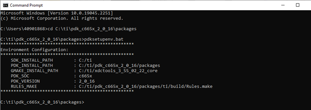
转至路径"C:\ti\pdk_c665x_2_0_16\packages "
运行"pdksetupenv.bat"
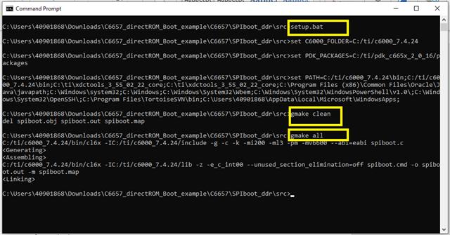
在文件 setup.bat 中设置 C6000编译器路径、并从 windows 命令行运行"setup.bat"文件。
设置 C6000_FOLDER=C:/ti/c6000_7.4.24
设置 pdk_package=C:/ti/pdk_c665x_2_0_16/packages
设置路径=%C6000_FOLDER%\bin;%path%
Step2:将目录更改为 src 并生成应用程序二进制文件:
步骤3:将 spidboot.out 复制到构建文件夹-"C6657_directROM_Boot_Examples\C6657\SPIboot_DDR\build"
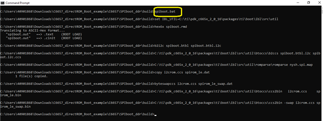
步骤4:将 spiboot.bat 文件中的 IBL_UTIL 路径设置为 Processor SDK 6.3 PDK 的 IBL utils 文件夹。
设置 IBL_UTIL=C:\ti\pdk_c665x_2_0_16\packages/ti\boot\IBL\src\util
hex6x spidboot.rmd
b2i2c spidboot.btbl spidboot.btbl.i2c
%IBL_UTIL%\btoccs\b2ccs spiboot.btbl.i2c spiboot.i2c.ccs
%IBL_UTIL%\romparse\romparse nysh.spi.map
复制 i2crom.CCS spirom_le.dat
byteswapccs i2crom.ccs spirom_le_swap.dat
%IBL_UTIL%\btoccs\ccs2bin i2crom.ccs spirom_le.bin
%IBL_UTIL%\btoccs\ccs2bin -swap i2crom.ccs spirom_le_swap.bin
步骤5:运行 spiboot.bat 文件以生成引导映像 spirom_le_swap.dat。
重要说明:在 CCS 中打开 spirom_le_swap.dat、如果值为" 0x51"、则将0x1F 偏移处的值更改为"00"
步骤6:将"spirom_le_swap.dAT"复制为"app.dAT"到"C6657_directROM_Boot_Examples\C6657\SPIboot_DDR\bin\flashwriter"
===========
为了确保 C6657内核上的 SPI 引导成功、
我包含了一段 GPIO 代码。 让我们在其中一个 GPIO 寄存器中设置一个值、并尝试使用 CCS 存储器窗口观察相同的值。
/* Copyright (C) 2014 Texas Instruments Incorporated - http://www.ti.com/
 *
 *
 *  Redistribution and use in source and binary forms, with or without
 *  modification, are permitted provided that the following conditions
 *  are met:
 *
 *    Redistributions of source code must retain the above copyright
 *    notice, this list of conditions and the following disclaimer.
 *
 *    Redistributions in binary form must reproduce the above copyright
 *    notice, this list of conditions and the following disclaimer in the
 *    documentation and/or other materials provided with the
 *    distribution.
 *
 *    Neither the name of Texas Instruments Incorporated nor the names of
 *    its contributors may be used to endorse or promote products derived
 *    from this software without specific prior written permission.
 *
 *  THIS SOFTWARE IS PROVIDED BY THE COPYRIGHT HOLDERS AND CONTRIBUTORS
 *  "AS IS" AND ANY EXPRESS OR IMPLIED WARRANTIES, INCLUDING, BUT NOT
 *  LIMITED TO, THE IMPLIED WARRANTIES OF MERCHANTABILITY AND FITNESS FOR
 *  A PARTICULAR PURPOSE ARE DISCLAIMED. IN NO EVENT SHALL THE COPYRIGHT
 *  OWNER OR CONTRIBUTORS BE LIABLE FOR ANY DIRECT, INDIRECT, INCIDENTAL,
 *  SPECIAL, EXEMPLARY, OR CONSEQUENTIAL DAMAGES (INCLUDING, BUT NOT
 *  LIMITED TO, PROCUREMENT OF SUBSTITUTE GOODS OR SERVICES; LOSS OF USE,
 *  DATA, OR PROFITS; OR BUSINESS INTERRUPTION) HOWEVER CAUSED AND ON ANY
 *  THEORY OF LIABILITY, WHETHER IN CONTRACT, STRICT LIABILITY, OR TORT
 *  (INCLUDING NEGLIGENCE OR OTHERWISE) ARISING IN ANY WAY OUT OF THE USE
 * OF THIS SOFTWARE, EVEN IF ADVISED OF THE POSSIBILITY OF SUCH DAMAGE. */

#include <stdio.h>
#include <string.h>
#include <stdint.h>
#include "tiboot.h"
#include "platform.h"

#pragma  DATA_SECTION (emif4Cfg, ".emif4Cfg")
const BOOT_EMIF4_TBL_T  emif4Cfg =  {

    BOOT_EMIF4_ENABLE_MSW_pllCtl          | \
    BOOT_EMIF4_ENABLE_MSW_sdRamTiming1    | \
    BOOT_EMIF4_ENABLE_MSW_sdRamTiming2    | \
    BOOT_EMIF4_ENABLE_MSW_sdRamTiming3    | \
    BOOT_EMIF4_ENABLE_MSW_ddrPhyCtl1      | \
    BOOT_EMIF4_ENABLE_MSW_sdRamRefreshCtl | \
	BOOT_EMIF4_ENABLE_MSW_sdRamOutImpdedCalCfg | \
	BOOT_EMIF4_ENABLE_MSW_sdRamConfig,

    BOOT_EMIF_ENABLE_SLSW_config0 | \
	BOOT_EMIF_ENABLE_SLSW_config6 | \
	BOOT_EMIF_ENABLE_SLSW_config7 | \
	BOOT_EMIF_ENABLE_SLSW_config8 | \
	BOOT_EMIF_ENABLE_SLSW_config9 | \
	BOOT_EMIF_ENABLE_SLSW_config10 | \
	BOOT_EMIF_ENABLE_SLSW_config18 | \
	BOOT_EMIF_ENABLE_SLSW_config19 | \
	BOOT_EMIF_ENABLE_SLSW_config20 | \
	BOOT_EMIF_ENABLE_SLSW_config22 | \
	BOOT_EMIF_ENABLE_SLSW_config12 | \
	BOOT_EMIF_ENABLE_SLSW_config23 | \
	BOOT_EMIF_ENABLE_SLSW_config21,      /* Config select slsw */
    0,      /* Config select lsw  */

    3,      /* pllPrediv  */
    40,     /* pllMult    */
    2,      /* pllPostDiv */

    0x62477AB2,  /* sdRamConfig */
    0,           /* sdRamConfig2, dont care*/
    0x0000144F,  /* sdRamRefreshCtl  */
    0x1333780C,  /* sdRamTiming1 */
    0x30717FE3,  /* sdRamTiming2 */
    0x559F86AF,  /* sdRamTiming3 */

    0,           /* lpDdrNvmTiming, dont care */
    0,           /* powerManageCtl, dont care */
    0,           /* iODFTTestLogic, dont care */
    0,           /* performCountCfg, dont care */
    0,           /* performCountMstRegSel, dont care */
    0,           /* readIdleCtl, dont care */
    0,           /* sysVbusmIntEnSet, dont care */
    0x70074c1f,  /* sdRamOutImpdedCalCfg, dont care */
    0,           /* tempAlterCfg, dont care */

    0x0010010F,  /* ddrPhyCtl1 */

    0,           /* ddrPhyCtl2, dont care */
    0,           /* priClassSvceMap, dont care */
    0,           /* mstId2ClsSvce1Map, dont care */
    0,           /* mstId2ClsSvce2Map, dont care */
    0,           /* eccCtl, dont care */
    0,           /* eccRange1, dont care */
    0,           /* eccRange2, dont care */
    0,           /* rdWrtExcThresh, dont care */

    0x87A0047F, 0, 0, 0, 0, 0, 0x33, 0x3A,
    0x2C, 0x2C, 0x21, 0, 0xAF00002, 0, 0, 0,
    0, 0, 0xB7, 0xB1, 0xA4, 0xA4, 0x98, 0x200,
    0, 0, 0, 0, 0, 0, 0, 0,

    0, 0, 0, 0, 0, 0, 0, 0,
    0, 0, 0, 0, 0, 0, 0, 0,
    0, 0, 0, 0, 0, 0, 0, 0,
    0, 0, 0, 0, 0, 0, 0, 0
};

#define GPIO_BASE (0x2320000)
#define GPIO_DIR_OFFSET (0x10)
#define GPIO_SETDATA_OFFSET (0x18)
#define GPIO_CLEARDATA_OFFSET (0x1C)

void testfunc();

void testfunc()
{

    while (1)
    {
        asm("   IDLE");

    }
}

void main(void)
{

    volatile uint32_t *reg_val;

     reg_val = (volatile uint32_t *)(GPIO_BASE + GPIO_DIR_OFFSET);
     // configure as output pin -- write 0 to the Direction register
     *reg_val &= ~ (1 << 8);


     reg_val = (volatile uint32_t *) (GPIO_BASE + GPIO_SETDATA_OFFSET);
     // Write value 1 in the set data register, so that Out data register will be 1
     *reg_val |= (1 << 8);
    testfunc();


}
替换 spiboot.c 中的上述代码
重复1-6中的所有步骤
===
====================================================================================================================================================================================================================================================================================================================================================================================================================================================================================================================================================================================================================================================================================
步骤:-- 使用 NOR 编写器实用程序将 SPI 引导代码刷写到 NOR 闪存中。
====================================================================================================================================================================================================================================================================================================================================================================================================================================================================================================================================================================================================================================================================================
现在,在步骤6之后,您将在--"C6657_directROM_Boot_Examples\C6657\SPIboot_DDR\bin\flashwriter"中放置 app.dat,其中 norwriter.out 存在。
====
1.在无引导模式下引导 EVM。
SW3{引脚0 - PIN8)= 10000000 (0 -开、1 -关)
SW5 (pin0 - PIN8)= 00000000
2.启动 CCS 并连接到 C6657内核0。 让 GEL 文件运行以初始化 PLL 和 DDR 存储器。
3.转到 bin/flashwriter,确保 norwriter_input_txt 指向"app.dAT"。
4.在 CCS 中、使用内存浏览器加载内存位置0x80000000。 加载 norwriter.out 文件并运行。
有关将引导映像刷写到 SPI 的完整说明、请参阅 Processor SDK 中 NORwriter 软件包中的 README (C6657)。
================================================================
执行 NOR 编写器.out 时输出控制台消息
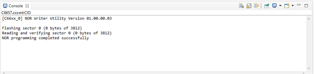
下面的视频给出了相同的刷写步骤。
e2e.ti.com/.../Nor_5F00_writer_5F00_Execution.mp4
===========
5.将 EVM 重新引导至直接 SPI 模式。 为此、请配置 DIP 开关:
SW3{引脚0 - PIN8)= 10110000 (0 -开、1 -关)
SW5 (pin0 - PIN8)= 00100000
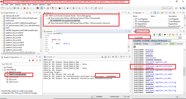
6.加电时使用 CCS 连接到 Core0,DDR 应由引导映像进行配置。
要进行测试、请连接到 GEM 内核0并导航到 CCS 中存储器浏览器中的地址0x8000000
和
它将在控制台中显示引导模式值为"6"-根据数据表显示 SPI 引导模式
7.进入内存浏览器窗口,将 GPIO 寄存器地址作为“0x2320000”输入。
请注意 、GPIO_bank 寄存器_out_data 中的值为"00000100"。
===================
此致
Shankari G
