
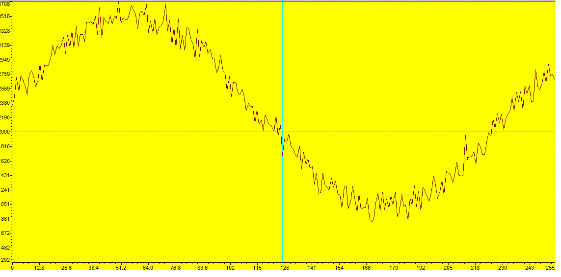
现象说明,采样256个点,内部基准电压,
有个奇怪的现象,内部基准正是1.5V,内部基准中是0.7V,不知道是不是正确,我的理解应该是内部基准正是3.0V,内部基准中是1.5V,才是正确,相关的资料里出也没有说明。请指教我这是出了什么问题

This thread has been locked.
If you have a related question, please click the "Ask a related question" button in the top right corner. The newly created question will be automatically linked to this question.
/**********************************************************************
* File: Adc.c
* Devices: TMS320F2833x
* Author: David M. Alter, Texas Instruments Inc.
* History:
* 12/18/07 - original (D. Alter)
**********************************************************************/
#include "DSP2833x_Device.h" // DSP2833x Headerfile Include File
#include "DSP2833x_Examples.h" // DSP2833x Examples Include File
//#define ADC_MODCLK 0x3 // HSPCLK = SYSCLKOUT/2*ADC_MODCLK2 = 150/(2*3) = 25.0 MHz
//#define ADC_CKPS 0x2 //=2 25/(2X2)=6.25MHZ ADC module clock = HSPCLK/1 = 25.5MHz/(1) = 25.0 MHz
//#define ADC_CPS 0x1 //=1 FCLK/2 =3.125MHZ
//#define ADC_SHCLK 0x8 // S/H width in ADC module periods S/H windows=(ADC_SHCLK+1)*ADC cycle
/**********************************************************************
* Function: InitAdc()
*
* Description: Initializes the ADC on the F2833x.
**********************************************************************/
void InitAdc(void)
{
///--- Reset the ADC module
AdcRegs.ADCTRL1.bit.RESET = 1; // Reset the ADC
// Must wait 2 ADCCLK periods for the reset to take effect. The ADC is
// already reset after a DSP reset, but this example is just showing good
// coding practice to reset the peripheral before configuring it (as you
// never know why the DSP has started the code over again from the
// beginning). Assuming a 12.5 MHz ADCCLK was previously configured, and
// a 150 MHz SYSCLKOUT, the wait period of 2 ADCCLK periods equates to 24
// CPU clocks. This is the example being used below.
asm(" RPT #22 || NOP"); // Must for ADC reset to take effect
EALLOW;
SysCtrlRegs.PCLKCR0.bit.ADCENCLK = 1;
ADC_cal();
// SysCtrlRegs.PCLKCR0.bit.ADCENCLK = 0;
EDIS;
// To powerup the ADC the ADCENCLK bit should be set first to enable
// clocks, followed by powering up the bandgap, reference circuitry, and ADC core.
// Before the first conversion is performed a 5ms delay must be observed
// after power up to give all analog circuits time to power up and settle
// Please note that for the delay function below to operate correctly the
// CPU_CLOCK_SPEED define statement in the DSP2833x_Examples.h file must
// contain the correct CPU clock period in nanoseconds.
// AdcRegs.ADCTRL3.all = 0x00E0; // Power up bandgap/reference/ADC circuits
// DELAY_US(ADC_usDELAY); //
//--- Call the ADC_cal() function located in the Boot ROM.
// ADC_cal_func_ptr is a macro defined in the file example_nonBios.h or
// example_BIOS.h (as may be the case for the example being used). This
// macro simply defines ADC_cal_func_ptr to be a function pointer to
// the correct address in the boot ROM.
// (*ADC_cal_func_ptr)();
//--- Select the ADC reference
AdcRegs.ADCREFSEL.bit.REF_SEL = 0; // 0=internal, 1=external
//--- Power-up the ADC
AdcRegs.ADCTRL3.all = 0x00EC; // Power-up reference and main ADC
// bit 15-8 0's: reserved
// bit 7-6 11: ADCBGRFDN, reference power, 00=off, 11=on
// bit 5 1: ADCPWDN, main ADC power, 0=off, 1=on
// bit 4-1 0110: ADCCLKPS, clock prescaler, FCLK=HSPCLK/(2*ADCCLKPS)
// bit 0 0: SMODE_SEL, 0=sequential sampling, 1=simultaneous sampling
DELAY_US(5000); // Wait 5ms before using the ADC
//--- Configure the other ADC register
AdcRegs.ADCMAXCONV.all = 0x0000;
// bit 15-7 0's: reserved
// bit 6-4 000: MAX_CONV2 value
// bit 3-0 0000: MAX_CONV1 value (0 means 1 conversion)
// Since we are only doing 1 conversion in the sequence, we only need to
// configure the ADCCHSELSEQ1 register, and only the CONV00 field. All
// other channel selection fields are don't cares in this example.
AdcRegs.ADCCHSELSEQ1.bit.CONV00 = 1; // Convert Channel 1
AdcRegs.ADCTRL1.all = 0x0710;
// bit 15 0: reserved
// bit 14 0: RESET, 0=no action, 1=reset ADC
// bit 13-12 00: SUSMOD, 00=ignore emulation suspend
// bit 11-8 0111: ACQ_PS (Acquisition), 0111 = 8 x ADCCLK
// bit 7 0: CPS (Core clock), 0: ADCCLK=FCLK/1, 1: ADCCLK=FCLK/2
// bit 6 0: CONT_RUN, 0=start/stop mode, 1=continuous run
// bit 5 0: SEQ_OVRD, 0=disabled, 1=enabled
// bit 4 1: SEQ_CASC, 0=dual sequencer, 1=cascaded sequencer
// bit 3-0 0000: reserved
AdcRegs.ADCTRL2.all = 0x0900;
// bit 15 0: ePWM_SOCB_SEQ, 0=no action
// bit 14 0: RST_SEQ1, 0=no action
// bit 13 0: SOC_SEQ1, 0=clear any pending SOCs
// bit 12 0: reserved
// bit 11 1: INT_ENA_SEQ1, 1=enable interrupt
// bit 10 0: INT_MOD_SEQ1, 0=int on every SEQ1 conv
// bit 9 0: reserved
// bit 8 1: ePWM_SOCA_SEQ1, 1=SEQ1 start from ePWM_SOCA trigger
// bit 7 0: EXT_SOC_SEQ1, 1=SEQ1 start from ADCSOC pin
// bit 6 0: RST_SEQ2, 0=no action
// bit 5 0: SOC_SEQ2, no effect in cascaded mode
// bit 4 0: reserved
// bit 3 0: INT_ENA_SEQ2, 0=int disabled
// bit 2 0: INT_MOD_SEQ2, 0=int on every other SEQ2 conv
// bit 1 0: reserved
// bit 0 0: ePWM_SOCB_SEQ2, 0=no action
//--- Enable the ADC interrupt
PieCtrlRegs.PIEIER1.bit.INTx6 = 0; // Enable ADCINT in PIE group 1
//IER |= 0x0001; // Enable INT1 in IER to enable PIE group
} // end InitAdc()
//--- end of file -----------------------------------------------------
void AdcSEQ_Iabc_Set(void)//外设ADC的SEQ1配置用来采样abc相负载电流
{
InitAdc();
EALLOW;
SysCtrlRegs.HISPCP.all = 0x33;//ADC_MODCLK; // HSPCLK = SYSCLKOUT/ADC_MODCLK
//PieVectTable.ADCINT=&ISRAdcSEQ;
//PieCtrlRegs.PIECTRL.bit.ENPIE = 1;
//PieCtrlRegs.PIEIER1.bit.INTx6 = 1; // Enable ADCINT in PIE group 1
//IER |= M_INT1;
EDIS;
AdcSEQ_Iabc_Stop();
// Secific ADC setup for this example:
AdcRegs.ADCTRL1.bit.ACQ_PS = ADC_SHCLK; // Sequential mode: Sample rate = 1/[(2+ACQ_PS)*ADC clock in ns]
// = 1/(3*40ns) =8.3MHz (for 150 MHz SYSCLKOUT)
// = 1/(3*80ns) =4.17MHz (for 100 MHz SYSCLKOUT)
// If Simultaneous mode enabled: Sample rate = 1/[(3+ACQ_PS)*ADC clock in ns]
AdcRegs.ADCTRL3.bit.ADCCLKPS = ADC_CKPS;
AdcRegs.ADCTRL1.bit.SEQ_CASC = 1; // 1 Cascaded mode 0 Dual_Sequencer Mode
AdcRegs.ADCTRL1.bit.CONT_RUN = 0; // 0 Start_Stop Run 1 Setup continuous run
AdcRegs.ADCTRL1.bit.SEQ_OVRD = 0; // Unable Sequencer override feature
AdcRegs.ADCTRL2.bit.INT_ENA_SEQ1=0;
AdcRegs.ADCTRL2.bit.INT_MOD_SEQ1= 0;
AdcRegs.ADCCHSELSEQ1.all = 0x8210;
AdcRegs.ADCCHSELSEQ2.all = 0xCBA9;//B4B3B2B1
AdcRegs.ADCCHSELSEQ3.all = 0x56ED;
AdcRegs.ADCCHSELSEQ4.all = 0x347;
AdcRegs.ADCMAXCONV.bit.MAX_CONV1 = 0x0E; //
}
void AdcSEQ_Iabc_Start(void)
{
AdcRegs.ADCTRL2.bit.SOC_SEQ1 = 0x1;
}
void AdcSEQ_Iabc_Stop(void)
{
AdcRegs.ADCTRL2.bit.RST_SEQ1= 0x1;
AdcRegs.ADCST.bit.INT_SEQ1_CLR = 1;
}
Uint16 AdcSEQ_Iabc_Result(ADC_SAMPLE *adresult)
{
Uint16 t=1000;
AdcSEQ_Iabc_Start();
while (AdcRegs.ADCST.bit.INT_SEQ1 == 0) //等待采样结果
{
t--;
if(t == 0) //等待时间
return 0xff;
}
// AdcRegs.ADCREFSEL.bit.REF_SEL = 0; // 0=internal, 1=external
// AdcRegs.ADCTRL1.bit.CONT_RUN = 0;
AdcSEQ_Iabc_Stop();
// //停止ADC
adresult->ua= ( (AdcRegs.ADCRESULT0)>>4);//* 3.0/4095.0;
adresult->ub= ( (AdcRegs.ADCRESULT1)>>4);//* 3.0/4095.0;
adresult->uc= ( (AdcRegs.ADCRESULT2)>>4);//* 3.0/4095.0;
adresult->ia_l= ( (AdcRegs.ADCRESULT3)>>4);//* 3.0/4095.0;
adresult->ib_l= ( (AdcRegs.ADCRESULT4)>>4);//* 3.0/4095.0;
adresult->ic_l= ( (AdcRegs.ADCRESULT5)>>4);//* 3.0/4095.0;
adresult->ia_o= ( (AdcRegs.ADCRESULT6)>>4);//* 3.0/4095.0;
adresult->ib_o= ( (AdcRegs.ADCRESULT7)>>4);//* 3.0/4095.0;
adresult->ic_o= ( (AdcRegs.ADCRESULT8)>>4);//* 3.0/4095.0;
adresult->ia_n= ( (AdcRegs.ADCRESULT9)>>4); //* 3.0/4095.0;
adresult->ib_n= ( (AdcRegs.ADCRESULT10)>>4);//* 3.0/4095.0;
adresult->ic_n= ( (AdcRegs.ADCRESULT11)>>4);//* 3.0/4095.0;
adresult->udc_pos= ( (AdcRegs.ADCRESULT13)>>4);//* 3.0/4095.0;//175 /1.16/1583
adresult->udc_neg= ( (AdcRegs.ADCRESULT14)>>4);//* 3.0/4095.0;//208V /1.36V /1856
adresult->tmptr= ( (AdcRegs.ADCRESULT12)>>4);//* 3.0/4095.0;
ua[uix] = adresult->ua;
ub[uix] = adresult->ub;
uc[uix] = adresult->uc;
ia[uix] = adresult->ia_o;
ib[uix] = adresult->ib_o;
ic[uix++] = adresult->ic_o;
}
