

Part Number: TMS320F28379D
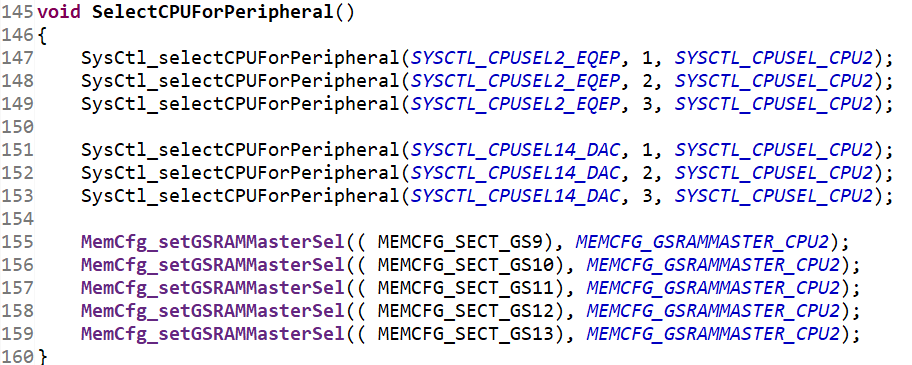
 The picture shows the configurations of Core 1 and Core 2. When using the TMS320F28379D chip, after I completed the program 固化 (program burning/flash programming) for Core 1 and Core 2, Core 1 was designed to handle status control-related processing, while Core 2 was responsible for generating motor waveform data points and outputting them through the DAC interface. However, it was found that after the program was burned into the flash, no waveform was output when sending commands via the serial port; nevertheless, the lighting test program burned into Core 1 functioned normally.
Subsequently, I wrote a simplified test program for burn verification: Core 2 was tasked with generating waveform data points, and Core 1 was responsible for command control. Under this setup, when control commands were sent via the serial port, Core 2 could output waveforms normally, and Core 1 could receive the commands and stop the waveform output.
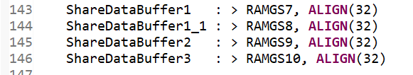
By checking the Flash address 0x082000 of both Core 1 and Core 2 using the MemoryBrowser tool, it was found that data was stored at this address for both cores, indicating that the program had been written into the Flash. However, the waveform generation program of Core 2 did not execute after the chip was powered on. What could be the possible causes of this phenomenon?

