Part Number: LAUNCHXL-F28P65X
例如我使用的是官方例程led_ex1_c28x_dual_blinky_cpu1和led_ex1_c28x_dual_blinky_cpu2。都使用LAUNCHXL-flash模式。在cpu1下载完程序之后,仿真cpu2程序就会出现以下错误:“C28xx_CPU1: If erase/program (E/P) operation is being done on one core, the other core should not execute from shared-RAM (SR) as they are used for the E/P code. User code execution from SR could commence after the selected flash banks are programmed.
C28xx_CPU1: Only CPU1 on-chip Flash Plugin can configure clock for CPU1, and CPU2 Flash operations. Plugin automatically configures PLL when CPU1 Flash operations are invoked. However, if users want to do only CPU2 Flash operations without doing a prior CPU1 operation in the current session, they should click on 'Configure Clock' button in CPU1's on-chip Flash Plugin before invoking CPU2 Flash operations. When this button is used, Flash Plugin will configure the clock for CPU1/CPU2 at 200MHz using INTOSC as the clock source. Plugin will leave PLL config like this and user application should configure the PLL as required by application.
C28xx_CPU1: Before doing any flash operations using the flash plugin, (a) Please select which flash banks should be mapped to which CPU (CPU1 vs CPU2) - This selection should be done in CPU1 flash plugin GUI. (b) Please select the flash banks that the user would like the flash plugin to erase (in the CPU1 flash plugin GUI and the CPU2 flash plugin GUI)
C28xx_CPU2: If erase/program (E/P) operation is being done on one core, the other core should not execute from shared-RAM (SR) as they are used for the E/P code. User code execution from SR could commence after the selected flash banks are programmed.
C28xx_CPU2: Only CPU1 on-chip Flash Plugin can configure clock for CPU1, and CPU2 Flash operations. Plugin automatically configures PLL when CPU1 Flash operations are invoked. However, if users want to do only CPU2 Flash operations without doing a prior CPU1 operation in the current session, they should click on 'Configure Clock' button in CPU1's on-chip Flash Plugin before invoking CPU2 Flash operations. When this button is used, Flash Plugin will configure the clock for CPU1/CPU2 at 200MHz using INTOSC as the clock source. Plugin will leave PLL config like this and user application should configure the PLL as required by application.
C28xx_CPU2: Before doing any flash operations using the flash plugin, (a) Please select which flash banks should be mapped to which CPU (CPU1 vs CPU2) - This selection should be done in CPU1 flash plugin GUI. (b) Please select the flash banks that the user would like the flash plugin to erase (in the CPU1 flash plugin GUI and the CPU2 flash plugin GUI)
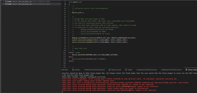
C28xx_CPU2: GSxMSEL register configured correctly
C28xx_CPU2: Flash Programmer: Error erasing Bank 0 FMSTAT (STATCMD on some devices) value = 65 (decimal). Operation Cancelled (0).
C28xx_CPU2: File Loader: Memory write failed: Unknown error
C28xx_CPU2: GEL: File: D:\projects\ti Project\led_ex1_c28x_dual_blinky_cpu2\CPU2_LAUNCHXL_FLASH\led_ex1_c28x_dual_blinky_cpu2.out: Load failed.
C28xx_CPU2: Error occurred during flash operation: Could not write register PC: target is not connected
C28xx_CPU2: Error occurred during flash operation: Could not write 0x000000@Program: target is not connected
C28xx_CPU2: Error occurred during flash operation: Cannot enable while the target is disconnected
C28xx_CPU2: Error occurred during flash operation: Could not read 0x0005F444@Data: target is not connected”