

各位大神好,28377D的DCSM从头到尾也看了两遍了,DCSM的寄存器也看了,然后就修改了以下的加密代码,使用的是controlSUITE里的blinky_with_dcsm_cpu01,相关内容如下:
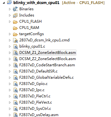
1、项目文件
2、2837xD_dcsm_lnk_cpu1.cmd 内容
MEMORY
{
PAGE 0 :  /* Program Memory */

   /* Z1 OTP.  LinkPointers */
   DCSM_OTP_Z1_LINKPOINTER   : origin = 0x78000, length = 0x00000C
   /* Z1 OTP.  PSWDLOCK/RESERVED */
   DCSM_OTP_Z1_PSWDLOCK	    : origin = 0x78010, length = 0x000004
   /* Z1 OTP.  CRCLOCK/RESERVED */
   DCSM_OTP_Z1_CRCLOCK	    : origin = 0x78014, length = 0x000004
   /* Z1 OTP.  RESERVED/BOOTCTRL */
   DCSM_OTP_Z1_BOOTCTRL	    : origin = 0x7801C, length = 0x000004

   /* DCSM Z1 Zone Select Contents (!!Movable!!) */
   /* Z1 OTP.  Z1 password locations / Flash and RAM partitioning */
   DCSM_ZSEL_Z1_P0	        : origin = 0x78020, length = 0x000010

   /* Z2 OTP.  LinkPointers */
   DCSM_OTP_Z2_LINKPOINTER	: origin = 0x78200, length = 0x00000C
   /* Z2 OTP.  GPREG1/GPREG2 */
   DCSM_OTP_Z2_GPREG	        : origin = 0x7820C, length = 0x000004
   /* Z2 OTP.  PSWDLOCK/RESERVED */
   DCSM_OTP_Z2_PSWDLOCK	    : origin = 0x78210, length = 0x000004
   /* Z2 OTP.  CRCLOCK/RESERVED */
   DCSM_OTP_Z2_CRCLOCK	    : origin = 0x78214, length = 0x000004
   /* Z2 OTP.  GPREG3/BOOTCTRL */
   DCSM_OTP_Z2_BOOTCTRL	    : origin = 0x7821C, length = 0x000004

   /* DCSM Z1 Zone Select Contents (!!Movable!!) */
   /* Z2 OTP.  Z2 password locations / Flash and RAM partitioning  */
   DCSM_ZSEL_Z2_P0	        : origin = 0x78220, length = 0x000010

}

SECTIONS
{
   dcsm_otp_z1_linkpointer 	: > DCSM_OTP_Z1_LINKPOINTER		PAGE = 0
   dcsm_otp_z1_pswdlock		: > DCSM_OTP_Z1_PSWDLOCK		PAGE = 0
   dcsm_otp_z1_crclock		: > DCSM_OTP_Z1_CRCLOCK			PAGE = 0
   dcsm_otp_z1_bootctrl		: > DCSM_OTP_Z1_BOOTCTRL		PAGE = 0
   dcsm_zsel_z1				: > DCSM_ZSEL_Z1_P0				PAGE = 0

   dcsm_otp_z2_linkpointer	: > DCSM_OTP_Z2_LINKPOINTER		PAGE = 0
   dcsm_otp_z2_pswdlock		: > DCSM_OTP_Z2_PSWDLOCK		PAGE = 0
   dcsm_otp_z2_crclock		: > DCSM_OTP_Z2_CRCLOCK			PAGE = 0
   dcsm_otp_z2_bootctrl		: > DCSM_OTP_Z2_BOOTCTRL		PAGE = 0
   dcsm_zsel_z2				: > DCSM_ZSEL_Z2_P0				PAGE = 0
}
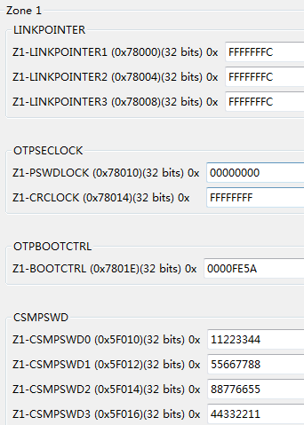
3、DCSM_Z1_ZoneSelectBlock.asm 文件内容
.sect "dcsm_otp_z1_linkpointer"
.long 0xFFFFFFFC ;Z1-LINKPOINTER1
.long 0x00000000 ;Reserved
.long 0xFFFFFFFC ;Z1-LINKPOINTER2
.long 0x00000000 ;Reserved
.long 0xFFFFFFFC ;Z1-LINKPOINTER3
.long 0x00000000 ;Reserved
.sect "dcsm_otp_z1_pswdlock"
.long 0x00000000 ;Z1-PSWDLOCK
.long 0x00000000 ;Reserved
.sect "dcsm_otp_z1_crclock"
.long 0xFFFFFFFF ;Z1-CRCLOCK
.long 0x00000000 ;Reserved
.sect "dcsm_otp_z1_bootctrl"
.long 0x00000000 ;Reserved
.long 0x0000FE5A ;Z1-BOOTCTRL
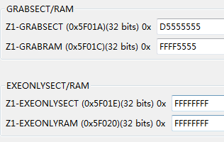
.sect "dcsm_zsel_z1"
.long 0xFFFFFF00 ;Z1-EXEONLYRAM
.long 0xFFFF8000 ;Z1-EXEONLYSECT
.long 0xFFFF5555 ;Z1-GRABRAM
.long 0xD5555555 ;Z1-GRABSECT
.long 0x11223344 ;Z1-CSMPSWD0 (LSW of 128-bit password)
.long 0x55667788 ;Z1-CSMPSWD1
.long 0x88776655 ;Z1-CSMPSWD2
.long 0x44332211 ;Z1-CSMPSWD3 (MSW of 128-bit password)
;----------------------------------------------------------------------
; For code security operation,after development has completed, prior to
; production, all other zone select block locations should be programmed
; to 0x0000 for maximum security.
; If the first zone select block at offset 0x10 is used, the section
;"dcsm_rsvd_z1" can be used to program these locations to 0x0000.
; This code is commented out for development.
; .sect "dcsm_rsvd_z1"
; .loop (1e0h)
; .int 0x0000
; .endloop
;//===========================================================================
;// End of file.
;//===========================================================================
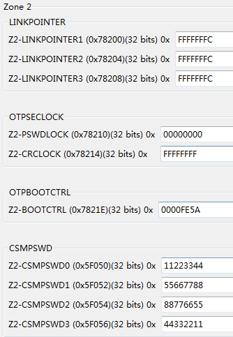
4、DCSM_Z2_ZoneSelectBlock.asm 文件内容
.sect "dcsm_otp_z2_linkpointer"
.long 0xFFFFFFFC ;Z2-LINKPOINTER1
.long 0x00000000 ;Reserved
.long 0xFFFFFFFC ;Z2-LINKPOINTER2
.long 0x00000000 ;Reserved
.long 0xFFFFFFFC ;Z2-LINKPOINTER3
.long 0x00000000 ;Reserved
.sect "dcsm_otp_z2_pswdlock"
.long 0x00000000 ;Z2-PSWDLOCK
.long 0x00000000 ;Reserved
.sect "dcsm_otp_z2_crclock"
.long 0xFFFFFFFF ;Z2-CRCLOCK
.long 0x00000000 ;Reserved
.sect "dcsm_otp_z2_bootctrl"
.long 0x00000000 ;Reserved
.long 0x0000FE5A ;Z2-BOOTCTRL
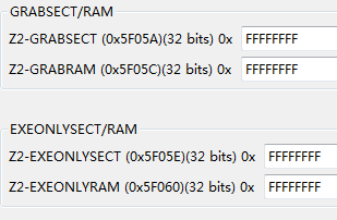
.sect "dcsm_zsel_z2"
.long 0xFFFFFFFF ;Z2-EXEONLYRAM
.long 0xFFFFFFFF ;Z2-EXEONLYSECT
.long 0xFFFFFFFF ;Z2-GRABRAM
.long 0xFFFFFFFF ;Z2-GRABSECT
.long 0x11223344 ;Z2-CSMPSWD0 (LSW of 128-bit password)
.long 0x55667788 ;Z2-CSMPSWD1
.long 0x88776655 ;Z2-CSMPSWD2
.long 0x44332211 ;Z2-CSMPSWD3 (MSW of 128-bit password)
;----------------------------------------------------------------------
; For code security operation,after development has completed, prior to
; production, all other zone select block locations should be programmed
; to 0x0000 for maximum security.
; If the first zone select block at offset 0x10 is used, the section
;"dcsm_rsvd_z2" can be used to program these locations to 0x0000.
; This code is commented out for development.
; .sect "dcsm_rsvd_z2"
; .loop (1e0h)
; .int 0x0000
; .endloop
;//===========================================================================
;// End of file.
;//===========================================================================
5、Target Properties
6、在烧写进去的时候,报警
C28xx_CPU1: GEL Output:
Memory Map Initialization Complete
C28xx_CPU1: If erase/program (E/P) operation is being done on one core, the other core should not execute from shared-RAM (SR) as they are used for the E/P code.  Also, CPU1 will be halted to determine SR ownership for the CPU which will run the Flash Plugin code, after which CPU1 will be set to run its application. User code execution from SR could commence after both flash banks are programmed.
C28xx_CPU1: Error during Flash programming (Flash algorithm returned error code). Operation cancelled.
C28xx_CPU1: File Loader: Memory write failed: Unknown error
C28xx_CPU1: GEL: File: E:\Software\NEEFLCT100100A-B01\DCDC-DCSM\v210\F2837xD_examples_Cpu1\blinky_with_DCSM\cpu01\ccs\CPU1_FLASH\blinky_with_dcsm_cpu01.out: Load failed.
请问下哪里出了问题呢? 谢谢了。
