This thread has been locked.

If you have a related question, please click the "Ask a related question" button in the top right corner. The newly created question will be automatically linked to this question.

TMS320F28035 关于cal触发问题

Other Parts Discussed in Thread: C2000WARE, TMS320F28035

我的芯片是TMS320F28035,我测试了C2000Ware_3_02_00_00这个库里面的cla_adc这个例程,然后发现那个adc触发是pwm周期内多次触发,而不是pwm一次,adc触发cla一次。我把代码贴出来

#include "DSP28x_Project.h" // Device Headerfile and Examples Include File
#include "CLAShared.h"
#include <string.h>
#include <stdint.h>

//
// Prototype statements
//
__interrupt void cla1_isr2(void);

//
// Globals
//
#pragma DATA_SECTION(ConversionCount, "Cla1ToCpuMsgRAM");
#pragma DATA_SECTION(VoltageCLA, "Cla1ToCpuMsgRAM");

Uint16 ConversionCount;
Uint16 LoopCount;
Uint16 VoltageCLA[NUM_DATA_POINTS];

extern Uint16 Cla1funcsLoadStart;
extern Uint16 Cla1funcsLoadSize;
extern Uint16 Cla1funcsRunStart;

void Gpio_select(void)
{
EALLOW;

GpioCtrlRegs.GPADIR.bit.GPIO12 = 0x01; // All outputs
GpioCtrlRegs.GPADIR.bit.GPIO24 = 0x01;
GpioCtrlRegs.GPBDIR.bit.GPIO34 = 0x01;

GpioDataRegs.GPADAT.bit.GPIO12 =0x01;
GpioDataRegs.GPADAT.bit.GPIO24 =0x01;
GpioDataRegs.GPBDAT.bit.GPIO34 =0x01;
EDIS;
}

void main(void)
{
Uint16 adc_tmp,adc_val;
InitSysCtrl();
DINT;
InitPieCtrl();

IER = 0x0000;
IFR = 0x0000;

InitPieVectTable();


EALLOW; // This is needed to write to EALLOW protected register
PieVectTable.CLA1_INT2 = &cla1_isr2;
EDIS; // This is needed to disable write to EALLOW protected registers

InitAdc(); // For this example, init the ADC
AdcOffsetSelfCal();

PieCtrlRegs.PIEIER11.bit.INTx2 = 1; // Enable INT 11.2 in PIE (CLA Task2)
IER |= M_INT11; // Enable CPU Interrupt 11
EINT; // Enable Global interrupt INTM
ERTM; // Enable Global realtime interrupt DBGM

memcpy((uint16_t *)&Cla1funcsRunStart,(uint16_t *)&Cla1funcsLoadStart,
(unsigned long)&Cla1funcsLoadSize);


EALLOW;
Cla1Regs.MVECT2 = (Uint16)((Uint32)&Cla1Task2 - (Uint32)&Cla1Prog_Start);
Cla1Regs.MVECT8 = (Uint16)((Uint32)&Cla1Task8 - (Uint32)&Cla1Prog_Start);

Cla1Regs.MPISRCSEL1.bit.PERINT2SEL = CLA_INT2_ADCINT2;

Cla1Regs.MMEMCFG.bit.PROGE = 1; // Map CLA program memory to the CLA
Cla1Regs.MCTL.bit.IACKE = 1; // Enable IACK to start tasks via software
Cla1Regs.MIER.all = (M_INT8 | M_INT2); // Enable Task 8 and Task 2
Cla1ForceTask8andWait(); // Force CLA task 8.
// This will initialize ConversionCount to zero

AdcRegs.ADCCTL1.bit.INTPULSEPOS = 0;

AdcRegs.INTSEL1N2.bit.INT2E = 1; //Enable ADCINT2
AdcRegs.INTSEL1N2.bit.INT2CONT = 0; //Disable ADCINT2 Continuous mode
AdcRegs.INTSEL1N2.bit.INT2SEL = 1; //setup EOC1 to trigger ADCINT2 to fire
AdcRegs.ADCSOC1CTL.bit.CHSEL = 2; //set SOC1 channel select to ADCINA2
AdcRegs.ADCSOC1CTL.bit.TRIGSEL = 5; //set SOC1 start trigger on EPWM1A

AdcRegs.ADCSOC1CTL.bit.ACQPS = 6;
EDIS;

InitEPwm1Gpio();
EALLOW;
SysCtrlRegs.PCLKCR0.bit.TBCLKSYNC = 0;
EDIS;

EPwm1Regs.AQCTLA.bit.ZRO = AQ_SET; // PWM toggle high/low
EPwm1Regs.AQCTLA.bit.CAU = AQ_CLEAR;


EPwm1Regs.ETSEL.bit.SOCAEN = 1; // Enable SOC on A group
EPwm1Regs.ETSEL.bit.SOCASEL = 4; // Select SOC from from CPMA on upcount
EPwm1Regs.ETPS.bit.SOCAPRD = 1; // Generate pulse on 1st event
EPwm1Regs.CMPA.half.CMPA = 0x2EE; // Set compare A value

EPwm1Regs.TBPRD = 0x5DC;

EPwm1Regs.TBCTL.bit.CTRMODE = 0; // count up and start
EALLOW;
SysCtrlRegs.PCLKCR0.bit.TBCLKSYNC = 1;
EDIS;

Gpio_select();
for(;;)
{
adc_val=ConversionCount;
adc_tmp=VoltageCLA[0];
LoopCount++;
}
}

__interrupt void cla1_isr2()
{
GpioDataRegs.GPATOGGLE.bit.GPIO24=1;
AdcRegs.ADCINTFLGCLR.bit.ADCINT2 = 1;
PieCtrlRegs.PIEACK.all = 0xFFFF;
}

这个代码我就是把pwm1a的信号输出,还有就是在__interrupt void cla1_isr2()这个中断里面翻转了一下IO,然后抓取了pwm的波形跟__interrupt void cla1_isr2()中断的波形,发现pwm输出是20khz,而中断的频率到了250khz,跟我的理解不一样啊,我的理解应该是pwm一个周期应该产生一次adc触发,cla收到adc触发后,在Cla1Task2这个任务里转换一次adc,然后产生__interrupt void cla1_isr2()中断告知cpu,不知道我的理解是否正确。我把波形贴出来,大神帮我看看,为什么实际产生的波形跟我的理解有误差呢?
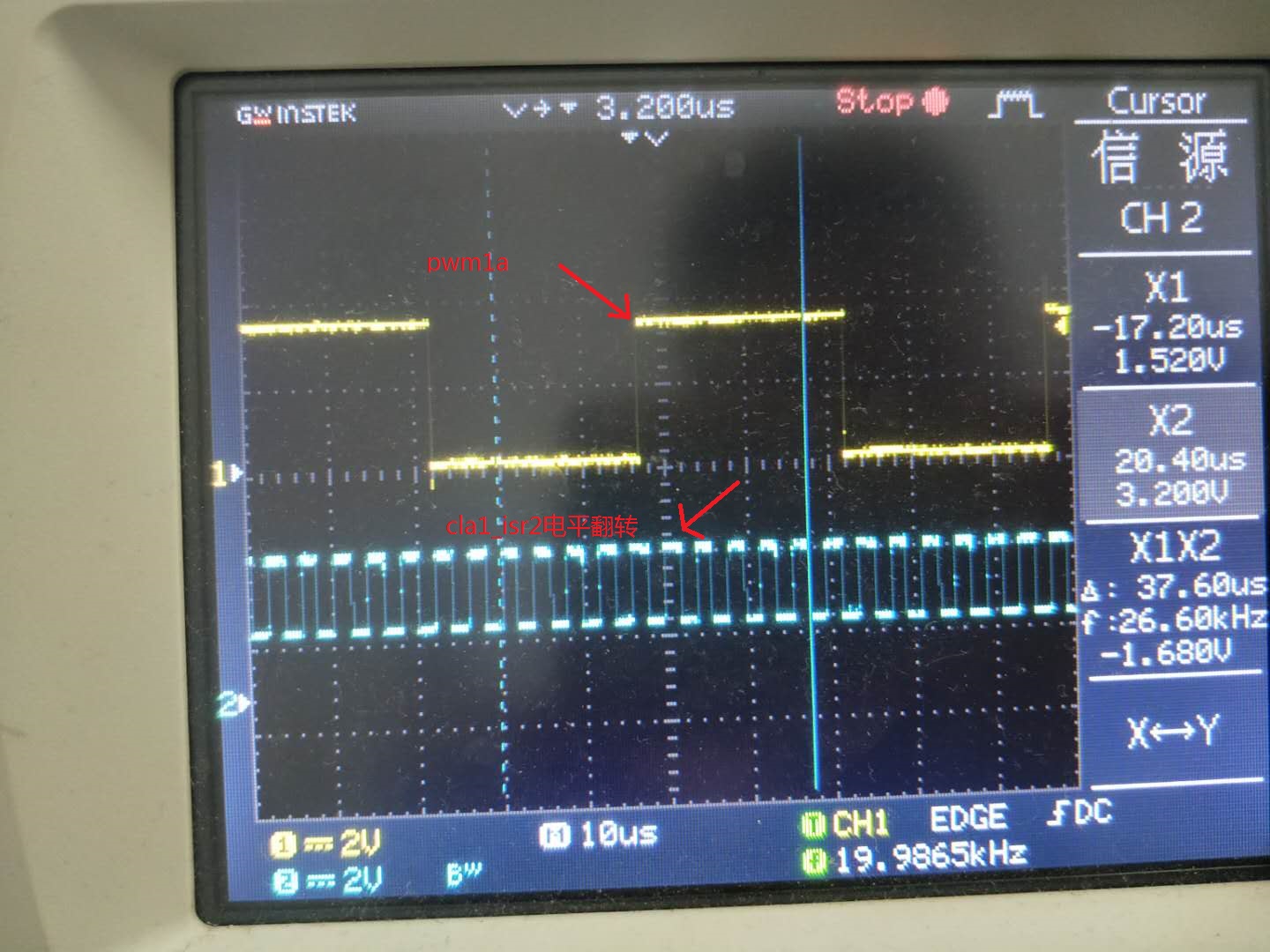
我的问题:

1、为什么那个__interrupt void cla1_isr2()中断不是pwm1a在一个周期内只产生1次?

  • 1、我不确定你测的GPIO波形是否正确?正常的GPIO波形应该是0~3.3V的,为什么你的波形幅值这么奇怪。。。
    2、例程里面采的是ADCINA2通道,把结果存到了ADCRESULT1的,这点没有问题啊
  • GPIO是正常的,那个波形是由于有led后跟一个限流电阻,我量的led端电压

    adcresult1问题我找到资料了,但是那个cal中断就不知道是为什么了

  • 没人回答么?自己顶一下
  • 而且频率的倍数也挺奇怪,你的程序中有哪些是频率相差12.5倍的吗?示波器设置正确吗?

  • 2us翻转一次,pwm是20K,那个cla中断产生的波形是250K,是相差12.5倍,这个是你们官方的程序,我只是增加了IO观测而已,来验证你们的资料说明,你们可以重现的,在程序里面我啥也没干。

  • 我的编译环境是ccs10 64位,你们可以自测一下
  • 好的,我会尽快测试后回复你
  • 我昨天测试了一下,确实GPIO的频率在250KHz左右(我测到的是252KHz)。我会跟其他工程师商量一下,看是否是测试方法不对,有结果了尽快回复给你。
  • 好的,我在你们的官网上,在Example_2803xAdcSoc这个工程上看到了

    // set SOC0 channel select to ADCINA4
    // (dummy sample for rev0 errata workaround)
    然后他的配置如下:

    AdcRegs.ADCSOC0CTL.bit.CHSEL = 4;
    AdcRegs.ADCSOC1CTL.bit.CHSEL = 4; //set SOC1 channel select to ADCINA4
    AdcRegs.ADCSOC2CTL.bit.CHSEL = 2; //set SOC2 channel select to ADCINA2
    AdcRegs.ADCSOC0CTL.bit.TRIGSEL = 5;
    AdcRegs.ADCSOC1CTL.bit.TRIGSEL = 5;
    AdcRegs.ADCSOC2CTL.bit.TRIGSEL = 5;


    AdcRegs.ADCSOC0CTL.bit.ACQPS = 6;
    AdcRegs.ADCSOC1CTL.bit.ACQPS = 6;
    AdcRegs.ADCSOC2CTL.bit.ACQPS = 6;

    这个ADCINA4居然被配置了两次,如果是配置两次的话,那个adc_isr(void)中断如果加入gpio测试信号的话,就跟pwm1A同步,如果屏蔽配置一次的话,那个在adc_isr(void)里面gpio的测试信号就是250khz,就是如果这样设置:

    //AdcRegs.ADCSOC0CTL.bit.CHSEL = 4;
    AdcRegs.ADCSOC1CTL.bit.CHSEL = 4; //set SOC1 channel select to ADCINA4
    AdcRegs.ADCSOC2CTL.bit.CHSEL = 2; //set SOC2 channel select to ADCINA2
    //AdcRegs.ADCSOC0CTL.bit.TRIGSEL = 5;
    AdcRegs.ADCSOC1CTL.bit.TRIGSEL = 5;
    AdcRegs.ADCSOC2CTL.bit.TRIGSEL = 5;


    //AdcRegs.ADCSOC0CTL.bit.ACQPS = 6;
    AdcRegs.ADCSOC1CTL.bit.ACQPS = 6;
    AdcRegs.ADCSOC2CTL.bit.ACQPS = 6;

    adc_isr(void)中断的gpio信号就是250khz,估计你们可能以前应该发现了这个问题,您可以参考下

  • 关于dummy采样,可以参考这个帖子:e2e.ti.com/.../2642290
    但是dummy采样跟CLA中断触发频率有什么关系,确实还没有证实过。我咨询了美国工程师,但是这几天正处美国劳动节放假,目前还没收到回复。。。
  • 好的,美国工程师有回复也发出来参考下
  • 好的,因为时差关系,预计得周二夜间才能有回复
  • 这是昨晚收到的来自美国工程师的回复:
    The errata is with regard to a correct/incorrect ADC Result. This should not impact the functionality/correctness of matching the PWM ISR.

    The ADCISR is configured later in the example based of EOC2(SOC2 End Of Conversion); this always happens.

    I would be careful here though, as I don't believe the ADC example code initializes the config registers to zero. Meaning, even if you clear it in the code and reload and run, the values in those registers for SOC0 could remain set from a previous run. I would manually clear them out to see if this resolves anything.

    I'm not sure why the frequency would be higher, the SOC is still dependent on the PWM as the trigger source.
    另一位CLA方面的专家表示需要结合ADC方面的专家一起讨论一下这个问题,可能需要一周的时间
  • 大神,美国工程师有回复了么?
  • 大神,美国工程师那边有回复了么?
  • 上面已经回复了,你先看一下。
  • 这是另一位工程师的回复:
    If I understand, the CLA has been removed from the problem. The ADC conversions are occurring faster than the PWM should trigger them. A few ideas to check:

    The code shows the configuration of ADCSOC1CTL. Can you check the configuration of ADCSOC0CTL, 2CTL and 3CTL? The goal is to make sure they are not configured to also react to the same SOC signal and thus starting additional conversions to over-sample the ADC input. (refer to page 498-499 of the Technical Reference Manual).
    It's possible to feed back ADCINT1/ADCINT2 to start another conversion. This configuration is controlled by the ADCINTSOCSEL1/2 registers and could cause a continuous stream of conversions.