This thread has been locked.
If you have a related question, please click the "Ask a related question" button in the top right corner. The newly created question will be automatically linked to this question.
Other Parts Discussed in Thread: UNIFLASH
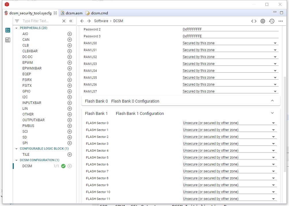
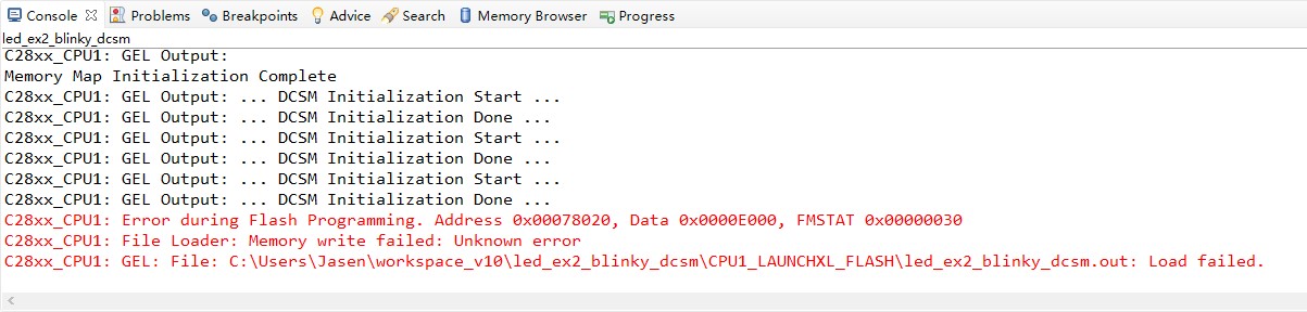
使用c2000 ware中dcsm_security_tool例程,将RAM LSx、Bank0左右扇区分配到Zone1、Bank1所有扇区分配到Zone2,分别设置了2个zone的密码,debug烧录完代码报下面错误。
附上生成的dcsm.asm和dcsm.cmd;---------------------------------------------------------------------- ; Zone 1 ;---------------------------------------------------------------------- .sect "dcsm_otp_z1_linkpointer" .retain .long 0x1FFFFFFF .long 0xFFFFFFFF ;Reserved .long 0x1FFFFFFF .long 0xFFFFFFFF ;Reserved .long 0x1FFFFFFF .long 0xFFFFFFFF ;Reserved .sect "dcsm_otp_z1_pswdlock" .retain .long 0xFB7FFFF0 .long 0x7FFFFFFF ;Reserved .sect "dcsm_otp_z1_crclock" .retain .long 0x4BFFFFFF .long 0x3FFFFFFF ;Reserved ;; .sect "dcsm_otp_z1_gpreg" ;; .retain ;; .long 0x5AFF1921 ;Z1OTP_BOOTPIN_CONFIG ;; .long 0x5AFFFFfF ;Z1OTP_GPREG2 ;; .sect "dcsm_otp_z1_bootctrl" ;; .retain ;; .long 0x00000000 ;Z1OTP_BOOTDEF_LOW ;; .long 0xFFFFFFFF ;Z1OTP_BOOTDEF_HIGH .sect "dcsm_zsel_z1" .retain .long 0x000000FF ;Z1-EXEONLYRAM .long 0x0000FFFF ;Z1-EXEONLYSECT .long 0x00005555 ;Z1-GRABRAM .long 0x55555555 ;Z1-GRABSECT .long 0xFFFFFFFF .long 0x47FFFFFF .long 0xFFFFFFFF .long 0xFFFFFFFE .sect "b1_dcsm_otp_z1_linkpointer" .retain .long 0x1FFFFFFF .long 0xFFFFFFFF ;Reserved .long 0x1FFFFFFF .long 0xFFFFFFFF ;Reserved .long 0x1FFFFFFF .long 0xFFFFFFFF ;Reserved .sect "b1_dcsm_zsel_z1" .retain .long 0xFFFFFFFF ;Reserved .long 0x0000FFFF ;Bank 1 Z1-EXEONLYSECT .long 0xFFFFFFFF ;Reserved .long 0xAAAAAAAA ;Bank 1 Z1-GRABSECT .long 0xFFFFFFFF ;Reserved .long 0xFFFFFFFF ;Reserved .long 0xFFFFFFFF ;Reserved .long 0xFFFFFFFF ;Reserved ;---------------------------------------------------------------------- ; For code security operation,after development has completed, prior to ; production, all other zone select block locations should be programmed ; to 0x0000 for maximum security. ; If the first zone select block at offset 0x10 is used, the section ; "dcsm_rsvd_z1" can be used to program these locations to 0x0000. ; This code is commented out for development. ; .sect "dcsm_rsvd_z1" ; .loop (1e0h) ; .int 0x0000 ; .endloop ;---------------------------------------------------------------------- ; Zone 2 ;---------------------------------------------------------------------- .sect "dcsm_otp_z2_linkpointer" .retain .long 0x1FFFFFFF .long 0xFFFFFFFF ;Reserved .long 0x1FFFFFFF .long 0xFFFFFFFF ;Reserved .long 0x1FFFFFFF .long 0xFFFFFFFF ;Reserved .sect "dcsm_otp_z2_pswdlock" .retain .long 0xBF7FFFF0 .long 0x77FFFFFF ;Reserved .sect "dcsm_otp_z2_crclock" .retain .long 0x0FFFFFFF .long 0x37FFFFFF ;Reserved ;; .sect "dcsm_otp_z2_gpreg" ;; .retain ;; .long 0x5AFF1921 ;Z2OTP_BOOTPIN_CONFIG ;; .long 0x5AFFFFfF ;Z2OTP_GPREG2 ;; .sect "dcsm_otp_z2_bootctrl" ;; .retain ;; .long 0x00000000 ;Z2OTP_BOOTDEF_LOW ;; .long 0xFFFFFFFF ;Z2OTP_BOOTDEF_HIGH .sect "dcsm_zsel_z2" .retain .long 0x000000FF ;z2-EXEONLYRAM .long 0x0000FFFF ;z2-EXEONLYSECT .long 0x0000AAAA ;z2-GRABRAM .long 0xAAAAAAAA ;z2-GRABSECT .long 0xFFFFFFFF .long 0xE3FFFFFF .long 0xFFFFFFFF .long 0xFFFFFFFE .sect "b1_dcsm_otp_z2_linkpointer" .retain .long 0x1FFFFFFF .long 0xFFFFFFFF ;Reserved .long 0x1FFFFFFF .long 0xFFFFFFFF ;Reserved .long 0x1FFFFFFF .long 0xFFFFFFFF ;Reserved .sect "b1_dcsm_zsel_z2" .retain .long 0xFFFFFFFF ;Reserved .long 0x0000FFFF ;Bank 1 Z2-EXEONLYSECT .long 0xFFFFFFFF ;Reserved .long 0x55555555 ;Bank 1 Z2-GRABSECT .long 0xFFFFFFFF ;Reserved .long 0xFFFFFFFF ;Reserved .long 0xFFFFFFFF ;Reserved .long 0xFFFFFFFF ;Reserved ;---------------------------------------------------------------------- ; For code security operation,after development has completed, prior to ; production, all other zone select block locations should be programmed ; to 0x0000 for maximum security. ; If the first zone select block at offset 0x10 is used, the section ; "dcsm_rsvd_z2" can be used to program these locations to 0x0000. ; This code is commented out for development. ; .sect "dcsm_rsvd_z2" ; .loop (1e0h) ; .int 0x0000 ; .endloop ;---------------------------------------------------------------------- ; End of file ;----------------------------------------------------------------------
/* this linker command file is to be included if user wants to use the DCSM feature on the device
 * DCSM  means Dual Zone Code Security Module.
 * This linker command file works as an addendum ot the already existing Flash/RAM linker command file
 * that the project has.
 * The sections in the *_ZoneSelectBlock.asm source file is linked as per the commands given in the file
 * NOTE - please note fill=0xFFFF, this helps if users include this file in the project by mistake and
 * doesn't provide the needed proper *_ZoneSelectBlock.asm sources .
 * Please refer to the Blinky DCSM example in the controlsuite examples for proper usage of this.
 *
 * Once users are confident that they want to program the passwords in OTP, the DSECT section type can be removed.
 *
*/

MEMORY
{
PAGE 0 :  /* Program Memory */

   /* Z1 OTP.  LinkPointers */
   DCSM_OTP_Z1_LINKPOINTER   : origin = 0x78000, length = 0x00000C
   /* Z1 OTP.  GPREG1/GPREG2 */
   DCSM_OTP_Z1_GPREG         : origin = 0x7800C, length = 0x000004
   /* Z1 OTP.  PSWDLOCK/RESERVED */
   DCSM_OTP_Z1_PSWDLOCK	    : origin = 0x78010, length = 0x000004
   /* Z1 OTP.  CRCLOCK/RESERVED */
   DCSM_OTP_Z1_CRCLOCK	    : origin = 0x78014, length = 0x000004
   /* Z1 OTP.  RESERVED/BOOTCTRL */
   DCSM_OTP_Z1_BOOTCTRL	    : origin = 0x7801C, length = 0x000004

   /* DCSM Z1 Zone Select Contents (!!Movable!!) */
   /* Z1 OTP.  Z1 password locations / Flash and RAM partitioning */
   DCSM_ZSEL_Z1_P0	        : origin = 0x78020, length = 0x000010

   /* Z2 OTP.  LinkPointers */
   DCSM_OTP_Z2_LINKPOINTER	: origin = 0x78200, length = 0x00000C
   /* Z2 OTP.  GPREG1/GPREG2 */
   DCSM_OTP_Z2_GPREG	        : origin = 0x7820C, length = 0x000004
   /* Z2 OTP.  PSWDLOCK/RESERVED */
   DCSM_OTP_Z2_PSWDLOCK	    : origin = 0x78210, length = 0x000004
   /* Z2 OTP.  CRCLOCK/RESERVED */
   DCSM_OTP_Z2_CRCLOCK	    : origin = 0x78214, length = 0x000004
   /* Z2 OTP.  GPREG3/BOOTCTRL */
   DCSM_OTP_Z2_BOOTCTRL	    : origin = 0x7821C, length = 0x000004

   /* DCSM Z1 Zone Select Contents (!!Movable!!) */
   /* Z2 OTP.  Z2 password locations / Flash and RAM partitioning  */
   DCSM_ZSEL_Z2_P0	        : origin = 0x78220, length = 0x000010

   /* BANK1 */
   /* B1 Z1 OTP.  LinkPointers */
   B1_DCSM_OTP_Z1_LINKPOINTER	: origin = 0x78400, length = 0x00000C

   /* DCSM B1 Z1 Zone Select Contents (!!Movable!!) */
   /* B1 Z1 OTP.  Flash partitioning */
   B1_DCSM_ZSEL_Z1_P0	        : origin = 0x78420, length = 0x000010

   /* B1 Z2 OTP.  LinkPointers */
   B1_DCSM_OTP_Z2_LINKPOINTER	: origin = 0x78600, length = 0x00000C

   /* DCSM B1 Z2 Zone Select Contents (!!Movable!!) */
   /* B1 Z2 OTP.  Flash partitioning  */
   B1_DCSM_ZSEL_Z2_P0	        : origin = 0x78620, length = 0x000010
}

SECTIONS
{
   dcsm_otp_z1_linkpointer 	: > DCSM_OTP_Z1_LINKPOINTER		PAGE = 0
   dcsm_otp_z1_gpreg        : > DCSM_OTP_Z1_GPREG		    PAGE = 0, type = DSECT
   dcsm_otp_z1_pswdlock		: > DCSM_OTP_Z1_PSWDLOCK		PAGE = 0
   dcsm_otp_z1_crclock		: > DCSM_OTP_Z1_CRCLOCK			PAGE = 0
   dcsm_otp_z1_bootctrl		: > DCSM_OTP_Z1_BOOTCTRL		PAGE = 0, type = DSECT
   dcsm_zsel_z1				: > DCSM_ZSEL_Z1_P0				PAGE = 0

   dcsm_otp_z2_linkpointer	: > DCSM_OTP_Z2_LINKPOINTER		PAGE = 0
   dcsm_otp_z2_gpreg        : > DCSM_OTP_Z2_GPREG		    PAGE = 0, type = DSECT
   dcsm_otp_z2_pswdlock		: > DCSM_OTP_Z2_PSWDLOCK		PAGE = 0
   dcsm_otp_z2_crclock		: > DCSM_OTP_Z2_CRCLOCK			PAGE = 0
   dcsm_otp_z2_bootctrl		: > DCSM_OTP_Z2_BOOTCTRL		PAGE = 0, type = DSECT
   dcsm_zsel_z2				: > DCSM_ZSEL_Z2_P0				PAGE = 0
   b1_dcsm_otp_z1_linkpointer 	: > B1_DCSM_OTP_Z1_LINKPOINTER		PAGE = 0
   b1_dcsm_zsel_z1				: > B1_DCSM_ZSEL_Z1_P0				PAGE = 0

   b1_dcsm_otp_z2_linkpointer	: > B1_DCSM_OTP_Z2_LINKPOINTER		PAGE = 0
   b1_dcsm_zsel_z2				: > B1_DCSM_ZSEL_Z2_P0				PAGE = 0
}

/*
//===========================================================================
// End of file.
//===========================================================================
*/
使用UniFlash读出来的GRABSECT/RAM值,跟生成的.asm中的不一样
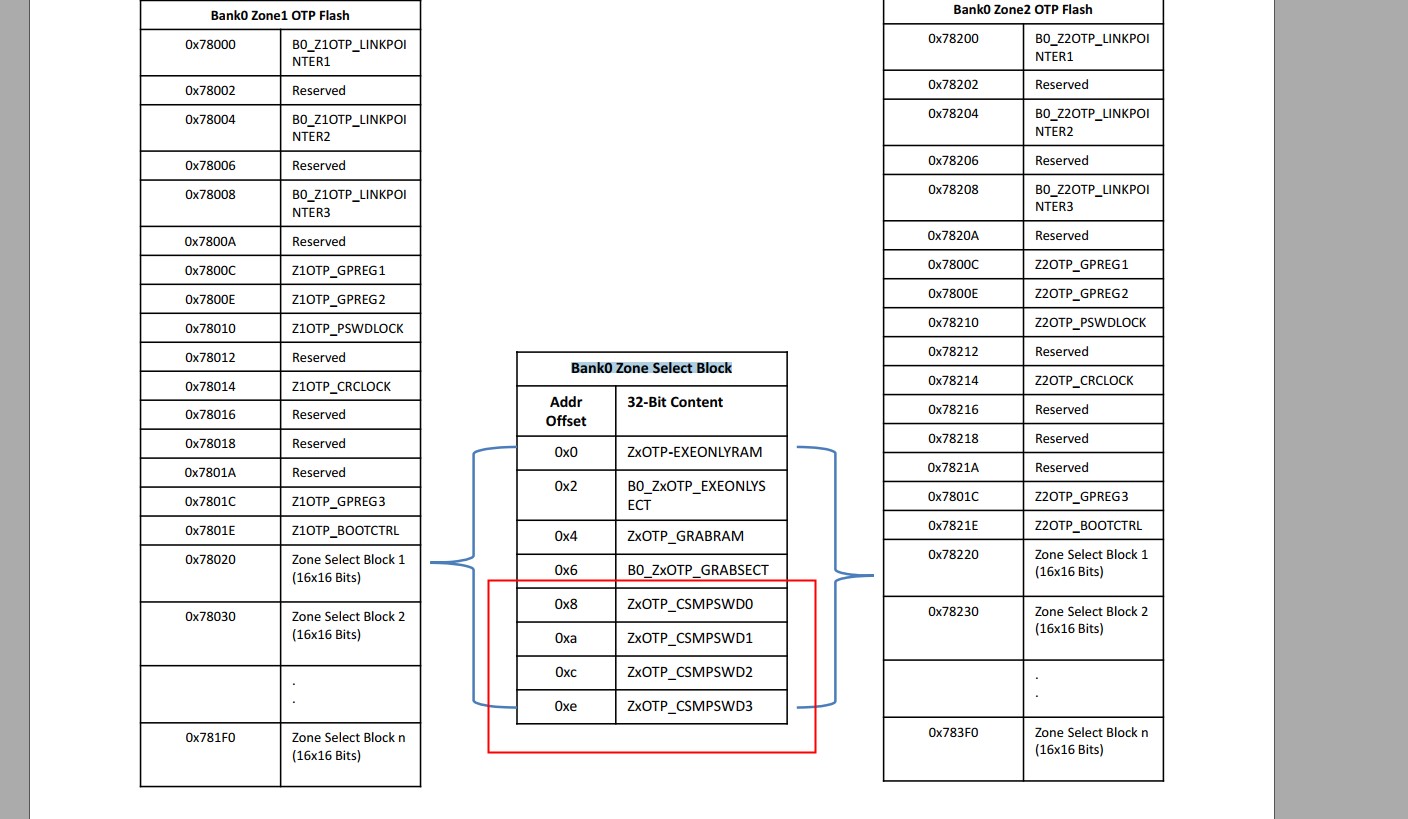
全新的dsp,错误发生在Flash programming 0x78020,是Bank0 Zone Select Block,密码在此区域。说明密码还没有写进去。
这个文章已经看过,F28004x的DCSM稍有不同,生成的DCSM asm cmd文件已经和TRM手册比对过,没发现问题
F28004x注意事项:
1、一旦设置了Zone密码,Flash、RAM LSx的访问就通过GRABRAM/GRABSECT去抓取,所以务必将所有Flash和RAM LSx进行划分加密。
2、GRABRAM/GRABSECT的配置是Zone1和Zone2的组合配置,不是单独的,错误配置将导致无妨访问。
3、在(存在Boot pin不确定的状态)硬件上测试,DCSM一直未成功写入,硬件的缺陷会影响DCSM的写入。
4、第一次烧录加密代码不需要任何额外的设置,后续需要在CCS工程属性->Debug->Flash Settings,CSMPSWD密码区域填入相应的密码。
或者使用UniFlash烧录之前,先通过Settings & Utilities CSMPSWD密码区域填入相应的密码。
5、尽量不要设置Boot ROM相关的,只能设置一次。