This thread has been locked.
If you have a related question, please click the "Ask a related question" button in the top right corner. The newly created question will be automatically linked to this question.
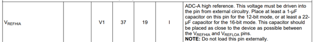
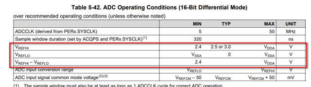
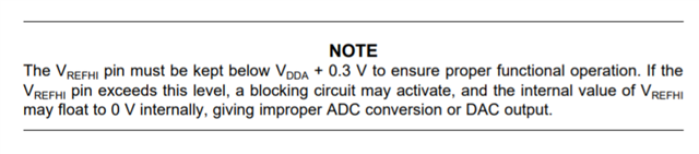
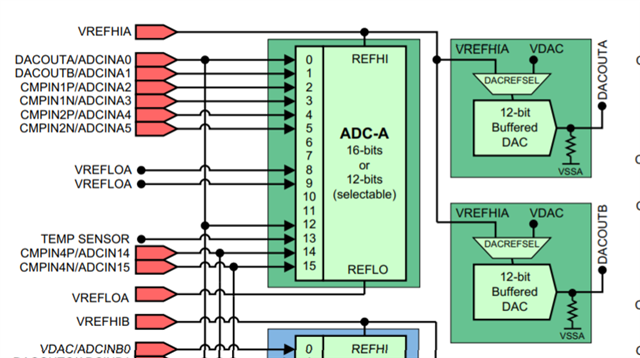
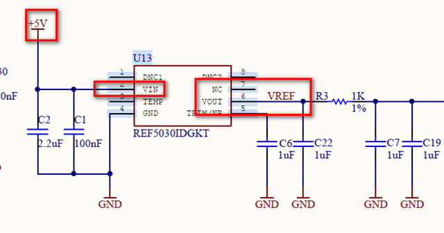
按照数据手册的说法,每个ADC都有一个VREFHI输入和一个VREFLO输入,用作比率参考。
这个VREFHI参考输入是怎么确定的呢?
整个具体的过程??
The ADCs are referenced to VREFHIx and VREFLOx pins
• VREFHIx pin voltage must be driven in externally
这个引脚是给哪个引脚参考电压呢
如之前所说,The ADCs are referenced to VREFHIx and VREFLOx pins.
这个电压可以作为ADC的参考电压,您可以看一下
https://www.ti.com.cn/cn/lit/ds/symlink/tms320f28379d.pdf
图 5-27. Analog Subsystem Block Diagram (337-Ball ZWT)
以及 图 5-30. ADC Module Block Diagram
您可以看一下 LaunchPad 的原理图
C:\ti\c2000\C2000Ware_x\boards\LaunchPads\LAUNCHXL_F28379D
您可以看到 VREF 由 U13 提供,然后通过 U11(馈送至 VREFHIA/C)和 U19(馈送至 VREFHIB/D)进行缓冲。