This thread has been locked.

If you have a related question, please click the "Ask a related question" button in the top right corner. The newly created question will be automatically linked to this question.

TMS320F28377D: 双核之间的通讯问题

Part Number: TMS320F28377D


28377D拥有两个DSP内核,那他们这两个内核是怎么进行通讯的呀,现在打算CPU1就进行AD采样计算之类,然后CPU2进行与外界的SCISPI通讯,那CPU2与外界通讯得到的数据怎么让CPU1可以读取呢,然后这个通讯与读取时间大致是多少呀,在官方例程里面我找到了三个例程,但是不明白每一个是什么意思
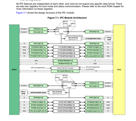
  ,模块是IPC这一块吗,

  • 是的,内部通信主要通过IPC模块。然后因为IPC其实是在两个shared message RAMs中的,所以访问速度很快,基本可以跟内部ram访问速度类似。

    官方提供的例程意思的话可以看一下每个例程main.c文件开头的注释,里面有说明工程的目的、需要观测的变量、需要的外部连接等等信息,比如第一个:

    工程的目的:

    //! This example tests all of the basic read/write CPU01 to CPU02 IPC Driver
    //! functions available in F2837xD_Ipc_Driver.c.
    //! The CPU01 project sends commands to the CPU02 project, which then processes
    //! the commands.
    //! The CPU02 project responds to the commands sent from the CPU01 project.
    //! Note that IPC INT0 and IPC INT1 are used for this example to process IPC
    //! commands.
    //!

    观测的变量
    //! \b Watch \b Variables \b for \b CPU01 : \n
    //! - ErrorCount - Counts # of errors
    //! - pusCPU01BufferPt - Stores 256 16-bit words block to write to CPU02
    //! - pusCPU02BufferPt - Points to beginning of 256 word block received
    //! back from CPU02
    //! - usWWord16 - 16-bit word to write to CPU02
    //! - ulWWord32 - 32-bit word to write to CPU02
    //! - usRWord16 - 16-bit word to read from CPU02
    //! - ulRWord32 - 32-bit word to read from CPU02
    //!
    //! \b Watch \b Variables \b for \b CPU02 : \n
    //! - ErrorFlag - Indicates an unrecognized command was sent from
    //! CPU01 to CPU02.

    无外部连接需要。