
请问由于这个问题导致的load不进flash,怎么处理,我用的是TI的LLC谐振开发套件,用的cmd文件是controlsuite中的F28027_FLASH_HVLLC.CMD.请TI员工帮帮忙啊,我一直弄不出来。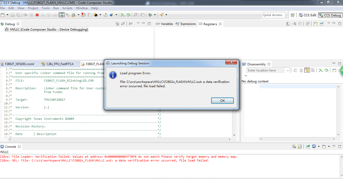

This thread has been locked.
If you have a related question, please click the "Ask a related question" button in the top right corner. The newly created question will be automatically linked to this question.
请问由于这个问题导致的load不进flash,怎么处理,我用的是TI的LLC谐振开发套件,用的cmd文件是controlsuite中的F28027_FLASH_HVLLC.CMD.请TI员工帮帮忙啊,我一直弄不出来。
我用的是controlsuite的CMD然后对照存储结构表对了,没问题的我把CMD文件贴出来啊,烦请指教
/*==================================================================================*/
/* User specific Linker command file for running from FLASH */
/*==================================================================================*/
/* FILE: F28027_FLASH_BlinkingLED.CMD */
/* */
/* Description: Linker command file for User custom sections targetted to run */
/* from FLASH. */
/* */
/* Target: TMS320F28027 */
/* */
/* Version: 1.1 */
/* */
/*----------------------------------------------------------------------------------*/
/* Copyright Texas Instruments �2009 */
/*----------------------------------------------------------------------------------*/
/* Revision History: */
/*----------------------------------------------------------------------------------*/
/* Date | Description */
/*----------------------------------------------------------------------------------*/
/* 04/24/09 | Release 1.1 */
/*----------------------------------------------------------------------------------*/
/* Define the memory block start/length for the F28022
PAGE 0 will be used to organize program sections
PAGE 1 will be used to organize data sections
Notes:
Memory blocks on F2802x are uniform (ie same
physical memory) in both PAGE 0 and PAGE 1.
That is the same memory region should not be
defined for both PAGE 0 and PAGE 1.
Doing so will result in corruption of program
and/or data.
The L0 memory block is mirrored - that is
it can be accessed in high memory or low memory.
For simplicity only one instance is used in this
linker file.
Contiguous SARAM memory blocks or flash sectors can be
be combined if required to create a larger memory block.
*/
MEMORY
{
PAGE 0:
/* Program Memory */
/* Memory (RAM/FLASH/OTP) blocks can be moved to PAGE1 for data allocation */
BOOT_RSVD : origin = 0x000000, length = 0x000050 /* Part of M0, BOOT rom will use this for stack */
progRAM : origin = 0x008000, length = 0x000800
OTP : origin = 0x3D7800, length = 0x000400 /* on-chip OTP */
FLASHD : origin = 0x3F0000, length = 0x002000 /* on-chip FLASH */
FLASHC : origin = 0x3F2000, length = 0x002000 /* on-chip FLASH */
FLASHA : origin = 0x3F6000, length = 0x001F80 /* on-chip FLASH */
CSM_RSVD : origin = 0x3F7F80, length = 0x000076 /* Part of FLASHA. Program with all 0x0000 when CSM is in use. */
BEGIN : origin = 0x3F7FF6, length = 0x000002 /* Part of FLASHA. Used for "boot to Flash" bootloader mode. */
CSM_PWL : origin = 0x3F7FF8, length = 0x000008 /* Part of FLASHA. CSM password locations in FLASHA */
IQTABLES : origin = 0x3FE000, length = 0x000B50 /* IQ Math Table in Boot */
IQTABLES2 : origin = 0x3FEB50, length = 0x00008C /* IQ Math Table in Boot */
IQTABLES3 : origin = 0x3FEBDC, length = 0x0000AA /* IQ Math Table in Boot */
BOOTROM : origin = 0x3FF27C, length = 0x000D44 /* Boot ROM */
RESET : origin = 0x3FFFC0, length = 0x000002 /* part of boot ROM */
VECTORS : origin = 0x3FFFC2, length = 0x00003E /* part of boot ROM */
PAGE 1 :
/* Data Memory */
/* Memory (RAM/FLASH/OTP) blocks can be moved to PAGE0 for program allocation */
/* Registers remain on PAGE1 */
RAMM0 : origin = 0x000050, length = 0x0003B0
RAMM1 : origin = 0x000400, length = 0x000400
dataRAM : origin = 0x008800, length = 0x000800
FLASHB : origin = 0x3F4000, length = 0x002000
}
SECTIONS
{
/* Allocate program areas: */
.cinit : > FLASHA, PAGE = 0
.pinit : > FLASHA, PAGE = 0
.text : > FLASHA, PAGE = 0
codestart : > BEGIN PAGE = 0
ramfuncs : LOAD = FLASHA,
RUN = progRAM,
LOAD_START(_RamfuncsLoadStart),
LOAD_END(_RamfuncsLoadEnd),
RUN_START(_RamfuncsRunStart),
PAGE = 0
csmpasswds : > CSM_PWL PAGE = 0
csm_rsvd : > CSM_RSVD PAGE = 0
/* Allocate uninitalized data sections: */
.stack : > RAMM0, PAGE = 1
.ebss : > dataRAM, PAGE = 1
.esysmem : > dataRAM, PAGE = 1
/* Initalized sections go in Flash */
/* For SDFlash to program these, they must be allocated to page 0 */
.econst : > FLASHA PAGE = 0
.switch : > FLASHA PAGE = 0
/* Allocate IQ math areas: */
IQmath : > FLASHA PAGE = 0 /* Math Code */
IQmathTables : > IQTABLES PAGE = 0, TYPE = NOLOAD /* Math Tables In ROM */
/* Uncomment the section below if calling the IQNexp() or IQexp()
functions from the IQMath.lib library in order to utilize the
relevant IQ Math table in Boot ROM (This saves space and Boot ROM
is 1 wait-state). If this section is not uncommented, IQmathTables2
will be loaded into other memory (SARAM, Flash, etc.) and will take
up space, but 0 wait-state is possible.
*/
/*
IQmathTables2 : > IQTABLES2, PAGE = 0, TYPE = NOLOAD
{
IQmath.lib<IQNexpTable.obj> (IQmathTablesRam)
}
*/
/* Uncomment the section below if calling the IQNasin() or IQasin()
functions from the IQMath.lib library in order to utilize the
relevant IQ Math table in Boot ROM (This saves space and Boot ROM
is 1 wait-state). If this section is not uncommented, IQmathTables2
will be loaded into other memory (SARAM, Flash, etc.) and will take
up space, but 0 wait-state is possible.
*/
/*
IQmathTables3 : > IQTABLES3, PAGE = 0, TYPE = NOLOAD
{
IQmath.lib<IQNasinTable.obj> (IQmathTablesRam)
}
*/
.reset : > RESET, PAGE = 0, TYPE = DSECT
vectors : > VECTORS PAGE = 0, TYPE = DSECT
}
SECTIONS
{
/************* DPLIB Sections C28x ************************/
/* ADCDRV_1ch section */
ADCDRV_1ch_Section : > dataRAM PAGE = 1
/* ADCDRV_4ch section */
ADCDRV_4ch_Section : > dataRAM PAGE = 1
/* CNTL_2P2Z section */
CNTL_2P2Z_Section : > dataRAM PAGE = 1
CNTL_2P2Z_InternalData : > dataRAM PAGE = 1
CNTL_2P2Z_Coef : > dataRAM PAGE = 1
/* CNTL_3P3Z section */
CNTL_3P3Z_Section : > dataRAM PAGE = 1
CNTL_3P3Z_InternalData : > dataRAM PAGE = 1
CNTL_3P3Z_Coef : > dataRAM PAGE = 1
/*DLOG_4CH section */
DLOG_4CH_Section : > dataRAM PAGE = 1
DLOG_BUFF : > dataRAM PAGE = 1
/*MATH_EMAVG section */
MATH_EMAVG_Section : > dataRAM PAGE = 1
/*PFC_ICMD section*/
PFC_ICMD_Section : > dataRAM PAGE = 1
/*PFC_INVSQR section*/
PFC_INVSQR_Section : > dataRAM PAGE = 1
/* PWMDRV_1ch driver section */
PWMDRV_1ch_Section : > dataRAM PAGE = 1
/* PWMDRV_1chHiRes driver section */
PWMDRV_1chHiRes_Section : > dataRAM PAGE = 1
/* PWMDRV_PFC2PhiL driver section */
PWMDRV_PFC2PhiL_Section : > dataRAM PAGE = 1
/* PWMDRV_PSFB driver section */
PWMDRV_PSFB_Section : > dataRAM PAGE = 1
/* PWMDRV_DualUpDwnCnt driver section */
PWMDRV_DualUpDwnCnt_Section : > dataRAM PAGE = 1
/* PWMDRV_ComplPairDB driver section */
PWMDRV_ComplPairDB_Section : > dataRAM PAGE = 1
/* ZeroNet_Section */
ZeroNet_Section : > dataRAM PAGE = 1
/* PWMDRV_1ch_UpCntDB_Compl driver section */
PWMDRV_LLC_1ch_UpCntDB_Compl_Section : > dataRAM PAGE = 1
/* PWMDRV_1ch_UpCntDB driver section */
PWMDRV_LLC_1ch_UpCntDB_Section : > dataRAM PAGE = 1
/* PWMDRV_LLC_ComplPairDB driver section */
PWMDRV_LLC_ComplPairDB_Section : > dataRAM PAGE = 1
}
