Part Number: LM3485
Hi Team,
I would like to add a little more information. The power supply settings are: voltage 23.5V, current limit 2.1A. The current is 2.1A when the host is charging. The test is as shown on the right, which meets the current limit requirements. The abnormal host test current fluctuates between 1.5A and 17A. After replacing U1, it returns to normal. Replace the defective U1 with a normal PCBA, and the abnormality is reproduced. Cross-verification shows that the defective follows the host.A few questions from your last question, please.
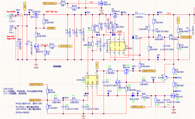
1、What is the Vout_set? --MCU控制此电路开关:0V FB受PWM控制,3.3V FB置高关闭此电路,正常工作时此脚0V
2、Please provide the complete schematic. [the connection from R11 is going to which point?]--工作状态参考我提供的简化原理图,R11未贴
3、what is the observed switching frequency?--50K,由MCU PWM-2提供,MMP-PWM未用。客户应用我理解为将此IC作为一个MOS驱动器在用
4、What is the inductor peak current?--约8A
5、C6 (CFF) should be in parallel to top feedback resistor. Currently there is R7 [150kohms] in series with CFF. What is the purpose? what is the purpose of this part? --不清楚客户应用目的,实测VFB 上升或下降沿顶部会轻微变缓(如右图),关于是否此点影响的我已排除,去掉C6电容或R14改10K(让FB高为2V,低为0.6V)不良现象仍在
6、Can you you reduce RADJ and check the limit?--R2 由110k改为10K,充电输入电流限制由1.6变到0.6A左右
电路图如下,NC空贴,输入23.5V限流2.1A,输出4串电池包约13V