

Hi i have a case designed as:
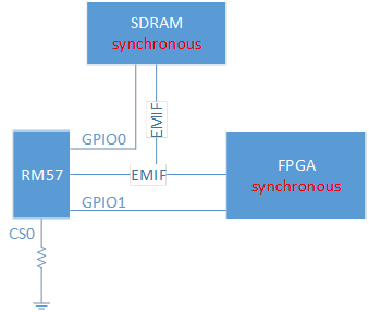
1: the circuit designed as above figure, GPIO0/GPIO1 as chip select signal, CS0 NC or to GND
2: FPGA and SDRAM connected with RM58 use EMIF and as synchronous communication
3: program executed from SDRAM, all code and data move into the SDRAM after system booted and initialed
if the solution designed as above , whether conflict between SDRAM with FPGA ?
and how do I design the circuit if i wanna fit the three conditions as mentioned above ?
