Other Parts Discussed in Thread: MSP430F5255
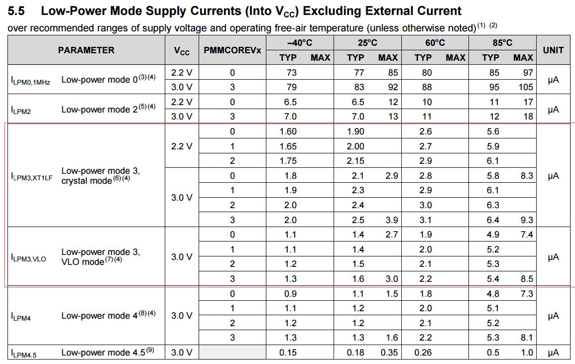
使用MSP430F5255单片机,外围电路全部没有焊接,只接了晶振和外部滤波电容。系统使用的是外部晶振12M,所有IO口配置为输出,并且拉低。进入LPM3模式,测得的电流有350uA,和datasheet里面说的25uA差了10倍,请问是什么问题?
Other Parts Discussed in Thread: MSP430F5255
使用MSP430F5255单片机,外围电路全部没有焊接,只接了晶振和外部滤波电容。系统使用的是外部晶振12M,所有IO口配置为输出,并且拉低。进入LPM3模式,测得的电流有350uA,和datasheet里面说的25uA差了10倍,请问是什么问题?