

Other Parts Discussed in Thread: MSP430FR6972
单片机型号MSP430FR6972
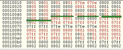
我想用ADC序列通道采样,通道0-1,触发DMA,把ADC采样的数据存到flash里去。单片机打断点的情况下,定时器每次触发ADC采样后,flash里更新了一个采样值,但是,实际情况是,采样完1s的数据,我看内存中的数据,两两是相同的,如下图,
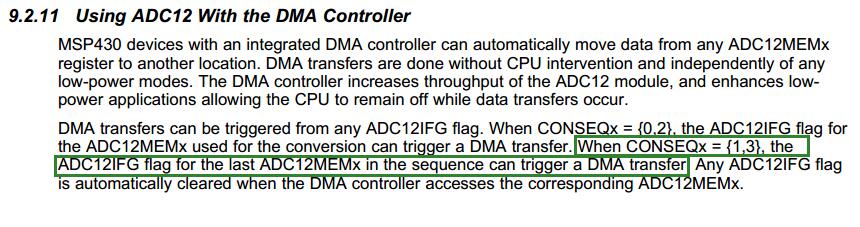
给我的感觉像两个ADC12IFGx标志触发了DMA,但是pdf也写了,由最后的ADC12IFGx触发DMA,
不知道是不是还需要别的设置。
做过的测试:
1.保留DMA0,注释DMA1,0-1通道序列采,值还是两两重复的。
2.保留DMA0,注释DMA1,0通道序列采样,值是正常的。
3.保留DMA0,注释DMA1,0-1通道单次序列采,flash里更新了两个值,的确触发了两次。
ADC和DMA配置如下:
void startADC(void)
{

      while(REFCTL0 & REFGENBUSY);              // If ref generator busy, WAIT
      REFCTL0 |= REFVSEL_2 | REFON;             // Select internal ref = 2.5V
                                                // Internal Reference ON
      // Configure ADC12
      ADC12CTL0 = ADC12ON | ADC12SHT0_2;        // Turn on ADC12, set sampling time 16 ADC12CLK
      ADC12CTL1 = ADC12SHP |ADC12SHS_1 | ADC12CONSEQ_3 ; // Timer_A TA0 CCR1触发采样,序列通道采样 0-1


      ADC12CTL3 = ADC12CSTARTADD_0;

      ADC12MCTL0 = ADC12INCH_2 | ADC12VRSEL_1 ;
      ADC12MCTL1 = ADC12INCH_3 | ADC12VRSEL_1 | ADC12EOS;

      //ADC12IER0 = ADC12IE1;

      ADC12CTL0 |= ADC12ENC | ADC12SC;

      // Configure DMA channel 0
    __data16_write_addr((unsigned short) &DMA0SA,(unsigned long) &ADC12MEM0);// Source block address
    __data16_write_addr((unsigned short) &DMA0DA,(unsigned long) 0x10000);// Destination address 0x10000
    DMA0SZ = 4000;                              // Block size
    DMACTL0 |= DMA0TSEL_26;                    //触发源选择ADC12采样完成

    DMA0CTL = DMADT_4 | DMASRCINCR_0 | DMADSTINCR_3; // Rpt, inc
    DMA0CTL |= DMAEN;                         // Enable DMA0

    // Configure DMA channel 1
    __data16_write_addr((unsigned short) &DMA1SA,(unsigned long) &ADC12MEM1);// Source block address
    __data16_write_addr((unsigned short) &DMA1DA,(unsigned long) 0x12000);// Destination address 0x12000
    DMA1SZ = 4000;                              // Block size
    DMACTL0 |= DMA1TSEL_26;                    //触发源选择ADC12采样完成
    DMA1CTL = DMADT_4 | DMASRCINCR_0 | DMADSTINCR_3; // Rpt, inc
    //DMA1CTL |= DMAEN;                         // Enable DMA1


}
