This thread has been locked.

If you have a related question, please click the "Ask a related question" button in the top right corner. The newly created question will be automatically linked to this question.

MSP430fr6989 硬件I2C

Other Parts Discussed in Thread: MSP430FR5969, MSP430FR6989

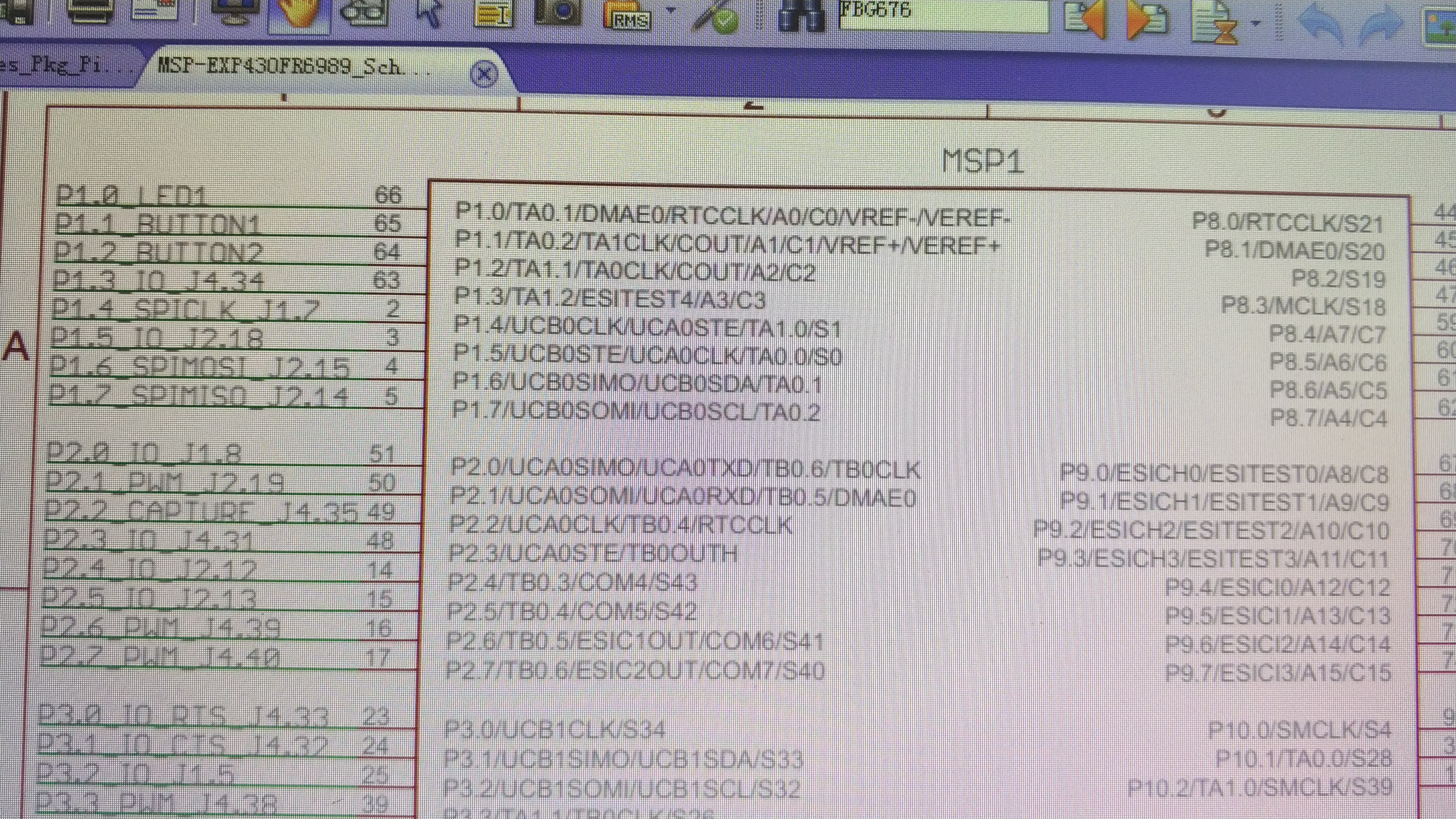
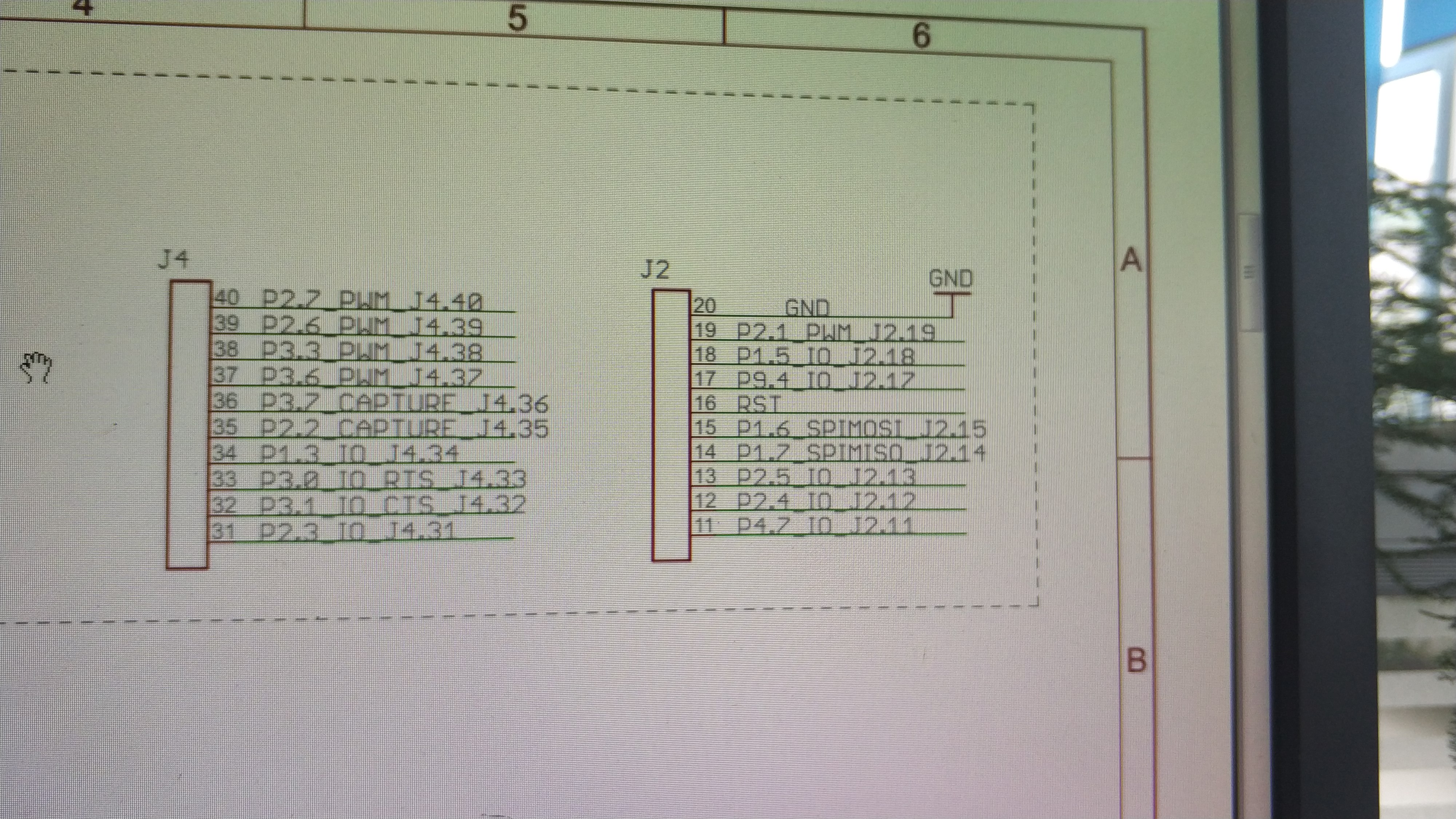
你好,想问一下,现在我手上有一块fr6989的launchpad,当我使用driverlib的硬件i2c的例子的时候,无论是主机还是从机模式都没反应,特别是主机模式发送,用示波器钩对应脚p1.6 1.7,一点反应都没有,跟踪内部寄存器,都是配置正确的,流程也是对的,就是不知道为什么一点反应都没有。1.6 1.7口通过普通输出IO翻转验证是好的。当从机的时候UCBBUSY就为1,ucsllow为0。外部已经加了上拉电阻。

  • 确认下,i2c配置完成以后p1.6和p1.7是否都是高电平

    正常情况下,i2c主机发送时,时钟线上能够看到时钟信号,数据线上能看到发的从地址

    i2c从机的UCBBUSY位应该是接收到起始信号后才会置位,接收到结束信号后后会清零

    硬件是开发板,应该没啥问题,还是怀疑配置上有错误

  • 谢谢解答。配置完后,需要设置内部上拉或者外部上拉才为高电平。然而发送时用示波器观察p1.7时钟脚确实没有信号,我用的是ti官方driverlib中的example,它是通过调用库函数初始化操作,我看了他的库函数确实配置流程是和userguide一致,跑起来后观察uscb中i2c相关所有寄存器配置值也是对的上的,非常奇怪,不会是他的库函数有问题吧。有没有代码参考一下

  • 谢谢解答。配置完后,需要设置内部上拉或者外部上拉才为高电平。然而发送时用示波器观察p1.7时钟脚确实没有信号一直为高,我用的是ti官方driverlib中的example,它是通过调用库函数初始化操作,我看了他的库函数确实配置流程是和userguide一致,跑起来后观察uscb中i2c相关所有寄存器配置值也是对的上的,非常奇怪,不会是他的库函数有问题吧。有没有代码参考一下

  • 你运行一下用寄存器操作的那个iic的例程试试。

    另外,你用的msp430ware是哪个版本?建议使用最新版本

    有条件的话,也可以换另外一个板子来实验下,看是不是硬件问题

  • 谢谢回答。

    我下的driverlib版本里都是库函数操作的,没有寄存器操作的,因为电脑用ccs一编译就卡死,只能用IAR。

    我已经再买了一块fr5969的launchpad,还没到。我主要是想用从机模式,第一次接触430平台,时间紧,只能用库函数的方式了。

    //----------------------------------这是driverlib中的例程-----------------------------------------------------//

    //--------------------------------------------------------------------------------------------------------------------//

    #include "driverlib.h"

    //*****************************************************************************
    //!
    //! Description: This demo connects two MSP430's via the I2C bus. The master
    //! reads from the slave. This is the SLAVE code. The TX data begins at 0
    //! and is incremented each time it is sent. A stop condition
    //! is used as a trigger to increment the outgoing data.
    //! The USCI_B0 TX interrupt is used to know
    //! when to TX.
    //! Tested on MSP430FR5969
    //!
    //! /|\ /|\
    // //! 10k 10k
    //! slave | | master
    //! ----------------- | | -----------------
    //! -|XIN P1.6/UCB0SDA|<-|----+->|P1.6/UCB0SDA XIN|-
    //! | | | | |
    //! -|XOUT | | | XOUT|-
    //! | P1.7/UCB0SCL|<-+------>|P1.7/UCB0SCL |
    //! | | | |
    //!
    //! This example uses the following peripherals and I/O signals. You must
    //! review these and change as needed for your own board:
    //! - I2C peripheral
    //! - GPIO Port peripheral (for I2C pins)
    //! - SCL2
    //! - SDA
    //!
    //! This example uses the following interrupt handlers. To use this example
    //! in your own application you must add these interrupt handlers to your
    //! vector table.
    //! - USCI_B0_VECTOR.
    //!
    //*****************************************************************************
    //*****************************************************************************
    //
    //Set the address for slave module. This is a 7-bit address sent in the
    //following format:
    //[A6:A5:A4:A3:A2:A1:A0:RS]
    //
    //A zero in the "RS" position of the first byte means that the master
    //transmits (sends) data to the selected slave, and a one in this position
    //means that the master receives data from the slave.
    //
    //*****************************************************************************
    #define SLAVE_ADDRESS 0x48

    uint8_t TXData = 0x00;

    void main(void)
    {
    WDT_A_hold(WDT_A_BASE);

    // Configure Pins for I2C
    //Set P1.6 and P1.7 as Secondary Module Function Input.
    /*

    * Select Port 1
    * Set Pin 6, 7 to input Secondary Module Function, (UCB0SIMO/UCB0SDA, UCB0SOMI/UCB0SCL).
    */
    GPIO_setAsPeripheralModuleFunctionInputPin(
    GPIO_PORT_P1,
    GPIO_PIN6 + GPIO_PIN7,
    GPIO_SECONDARY_MODULE_FUNCTION
    );

    /*
    * Disable the GPIO power-on default high-impedance mode to activate
    * previously configured port settings
    */
    PMM_unlockLPM5();

    // eUSCI configuration
    EUSCI_B_I2C_initSlaveParam param = {0};
    param.slaveAddress = SLAVE_ADDRESS;
    param.slaveAddressOffset = EUSCI_B_I2C_OWN_ADDRESS_OFFSET0;
    param.slaveOwnAddressEnable = EUSCI_B_I2C_OWN_ADDRESS_ENABLE;
    EUSCI_B_I2C_initSlave(EUSCI_B0_BASE, &param);

    //Enable I2C Module to start operations
    EUSCI_B_I2C_enable(EUSCI_B0_BASE);

    EUSCI_B_I2C_clearInterrupt(EUSCI_B0_BASE,
    EUSCI_B_I2C_TRANSMIT_INTERRUPT0 +
    EUSCI_B_I2C_STOP_INTERRUPT
    );

    EUSCI_B_I2C_enableInterrupt(EUSCI_B0_BASE,
    EUSCI_B_I2C_TRANSMIT_INTERRUPT0 +
    EUSCI_B_I2C_STOP_INTERRUPT
    );

    __bis_SR_register(CPUOFF + GIE); // Enter LPM0 w/ interrupts
    __no_operation();
    }

    //******************************************************************************
    //
    //This is the USCI_B0 interrupt vector service routine.
    //
    //******************************************************************************
    #if defined(__TI_COMPILER_VERSION__) || defined(__IAR_SYSTEMS_ICC__)
    #pragma vector=USCI_B0_VECTOR
    __interrupt
    #elif defined(__GNUC__)
    __attribute__((interrupt(USCI_B0_VECTOR)))
    #endif
    void USCIB0_ISR(void)
    {
    switch(__even_in_range(UCB0IV,0x1E))
    {
    case 0x00: break; // Vector 0: No interrupts break;
    case 0x02: break; // Vector 2: ALIFG
    case 0x04: break; // Vector 4: NACKIFG
    case 0x06: break; // Vector 6: STTIFG
    case 0x08: // Vector 8: STPIFG
    TXData++;
    break;
    case 0x0a: break; // Vector 10: RXIFG3 break;
    case 0x0c: break; // Vector 14: TXIFG3 break;
    case 0x0e: break; // Vector 16: RXIFG2 break;
    case 0x10: break; // Vector 18: TXIFG2 break;
    case 0x12: break; // Vector 20: RXIFG1 break;
    case 0x14: break; // Vector 22: TXIFG1 break;
    case 0x16: break; // Vector 24: RXIFG0 break;
    case 0x18:
    EUSCI_B_I2C_slavePutData(EUSCI_B0_BASE,
    TXData
    );
    break; // Vector 26: TXIFG0 break;
    case 0x1a: break; // Vector 28: BCNTIFG break;
    case 0x1c: break; // Vector 30: clock low timeout break;
    case 0x1e: break; // Vector 32: 9th bit break;
    default: break;
    }
    }

    //-------------------------------------------------------------------------------------------------------------//

    //----------------------------------这是库函数定义-----------------------------------------------------//

    //-------------------------------------------------------------------------------------------------------------//

    void EUSCI_B_I2C_initSlave(uint16_t baseAddress,
    EUSCI_B_I2C_initSlaveParam *param)
    {
    //Disable the USCI module
    HWREG16(baseAddress + OFS_UCBxCTLW0) |= UCSWRST;

    //Clear USCI master mode
    HWREG16(baseAddress + OFS_UCBxCTLW0) &= ~UCMST;

    //Configure I2C as Slave and Synchronous mode
    HWREG16(baseAddress + OFS_UCBxCTLW0) |= UCMODE_3 + UCSYNC;

    //Set up the slave address.
    HWREG16(baseAddress + OFS_UCBxI2COA0 + param->slaveAddressOffset)
    = param->slaveAddress + param->slaveOwnAddressEnable;
    }

    //-------------------------------------------------------------------------------------------------------------//

    void EUSCI_B_I2C_enable(uint16_t baseAddress)
    {
    //Reset the UCSWRST bit to enable the USCI Module
    HWREG16(baseAddress + OFS_UCBxCTLW0) &= ~(UCSWRST);
    }

    //-------------------------------------------------------------------------------------------------------------//

    void EUSCI_B_I2C_disable(uint16_t baseAddress)
    {
    //Set the UCSWRST bit to disable the USCI Module
    HWREG16(baseAddress + OFS_UCBxCTLW0) |= UCSWRST;
    }

    //-------------------------------------------------------------------------------------------------------------//

    void EUSCI_B_I2C_enableInterrupt(uint16_t baseAddress,
    uint16_t mask)
    {
    //Enable the interrupt masked bit
    HWREG16(baseAddress + OFS_UCBxIE) |= mask;
    }

    //-------------------------------------------------------------------------------------------------------------//

    void EUSCI_B_I2C_disableInterrupt(uint16_t baseAddress,
    uint16_t mask)
    {
    //Disable the interrupt masked bit
    HWREG16(baseAddress + OFS_UCBxIE) &= ~(mask);
    }

    //-------------------------------------------------------------------------------------------------------------//

    void EUSCI_B_I2C_clearInterrupt(uint16_t baseAddress,
    uint16_t mask)
    {
    //Clear the I2C interrupt source.
    HWREG16(baseAddress + OFS_UCBxIFG) &= ~(mask);
    }

  • 下载近板子时,已经将target改成msp430fr6989了

  • i2c配置完成后,在不通信的时候,时钟线和数据线一定是高电平,这点没有异议,是不需要做内部上拉的,希望仔细看一下开发板电路图,这两根线外部是否有上拉电阻,是否上拉到同一个电源上,我用5739的开发板它就没有外部上拉,是不可以进行i2c通信的

  • 板子上两个脚是直接引出到j2插针上,我不外挂上拉时,引脚为低电平

  • 那和我5739的开发板是一样的,没有上拉,是做不了i2c通信的,如果用外部的板子上拉要注意和单片机的电源电压保持一致,否则也可能带来问题,最好的还是用4.7k电阻上拉到单片机的Vcc

  • fr6989的launchpad P1.6,P1.7没有上拉电阻,做不了I2C,要做硬件I2C的话,data和clock一定要上拉,一般是4.7K

  • 然而外部添加了上拉电阻依然没有反应啊。