If you have a related question, please click the "Ask a related question" button in the top right corner. The newly created question will be automatically linked to this question.
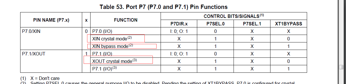
When XT1BYPASS is set, XT1 circuits are automatically powered down. Input signal is a digital square wave with parametrics defined in
the Schmitt-trigger Inputs section of this data sheet
您可以看一下 第5.2.4给出的说明
On many devices, the XT1 pins are shared with general-purpose I/O ports (refer to the device-specific data sheet for availability). At power up, the default operation is XT1, LF mode of operation. However, for devices that have XT1 shared with general-purpose I/O ports, XT1 will remain disabled until the ports shared with XT1 are configured for XT1 operation. The configuration of the shared I/O is determined by the PxSEL bit associated with XIN and the XT1BYPASS bit. Setting the PxSEL bit causes the XIN and XOUT ports to be configured for XT1 operation. If XT1BYPASS is also set, XT1 is configured for bypass mode of operation, and the oscillator associated with XT1 is powered down. In bypass mode of operation, XIN can accept an external clock input signal and XOUT is configured as a general-purpose I/O. The PxSEL bit associated with XOUT is a don't care. If the PxSEL bit associated with XIN is cleared, both XIN and XOUT ports are configured as general-purpose I/Os, and XT1 is disabled.