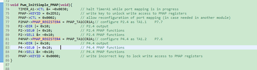
使用PMAP配置P2.4和P4.4为TA1.1和TA1.2功能配置电机,P2.4配置成功,出现了PWM波形,但是P4.4配置失败,想知道是什么原因:
This thread has been locked.
If you have a related question, please click the "Ask a related question" button in the top right corner. The newly created question will be automatically linked to this question.
使用PMAP配置P2.4和P4.4为TA1.1和TA1.2功能配置电机,P2.4配置成功,出现了PWM波形,但是P4.4配置失败,想知道是什么原因:
// RobotArmmain.c
// Runs on MSP432
// Basic test functionality for three-servo robot arm.
// Daniel and Jonathan Valvano
// November 16, 2018
/* This example accompanies the books
"Embedded Systems: Introduction to the MSP432 Microcontroller",
ISBN: 978-1512185676, Jonathan Valvano, copyright (c) 2018
"Embedded Systems: Real-Time Interfacing to the MSP432 Microcontroller",
ISBN: 978-1514676585, Jonathan Valvano, copyright (c) 2018
"Embedded Systems: Real-Time Operating Systems for ARM Cortex-M Microcontrollers",
ISBN: 978-1466468863, , Jonathan Valvano, copyright (c) 2018
For more information about my classes, my research, and my books, see
http://users.ece.utexas.edu/~valvano/
Simplified BSD License (FreeBSD License)
Copyright (c) 2018, Jonathan Valvano, All rights reserved.
Redistribution and use in source and binary forms, with or without modification,
are permitted provided that the following conditions are met:
1. Redistributions of source code must retain the above copyright notice,
this list of conditions and the following disclaimer.
2. Redistributions in binary form must reproduce the above copyright notice,
this list of conditions and the following disclaimer in the documentation
and/or other materials provided with the distribution.
THIS SOFTWARE IS PROVIDED BY THE COPYRIGHT HOLDERS AND CONTRIBUTORS "AS IS"
AND ANY EXPRESS OR IMPLIED WARRANTIES, INCLUDING, BUT NOT LIMITED TO, THE
IMPLIED WARRANTIES OF MERCHANTABILITY AND FITNESS FOR A PARTICULAR PURPOSE
ARE DISCLAIMED. IN NO EVENT SHALL THE COPYRIGHT OWNER OR CONTRIBUTORS BE
LIABLE FOR ANY DIRECT, INDIRECT, INCIDENTAL, SPECIAL, EXEMPLARY, OR CONSEQUENTIAL
DAMAGES (INCLUDING, BUT NOT LIMITED TO, PROCUREMENT OF SUBSTITUTE GOODS OR SERVICES;
LOSS OF USE, DATA, OR PROFITS; OR BUSINESS INTERRUPTION) HOWEVER CAUSED
AND ON ANY THEORY OF LIABILITY, WHETHER IN CONTRACT, STRICT LIABILITY,
OR TORT (INCLUDING NEGLIGENCE OR OTHERWISE) ARISING IN ANY WAY OUT OF THE
USE OF THIS SOFTWARE, EVEN IF ADVISED OF THE POSSIBILITY OF SUCH DAMAGE.
The views and conclusions contained in the software and documentation are
those of the authors and should not be interpreted as representing official
policies, either expressed or implied, of the FreeBSD Project.
*/
// Negative logic bump sensors
// P4.7 Bump5, left side of robot
// P4.6 Bump4
// P4.5 Bump3
// P4.3 Bump2
// P4.2 Bump1
// P4.0 Bump0, right side of robot
// The servos exceed the current limitation of standard USB, so when they
// are in use, the system must be powered with a bench power supply or
// the Pololu #3543 Motor Driver and Power Distribution Board.
// Pololu #3543 Vreg (5V regulator output) connected to all three Pololu #136 GP2Y0A21YK0F Vcc's (+5V) and MSP432 +5V (J3.21)
// Pololu #3543 Vreg (5V regulator output) connected to positive side of three 10 uF capacitors physically near the sensors
// Pololu ground connected to all three Pololu #136 GP2Y0A21YK0F grounds and MSP432 ground (J3.22)
// Pololu ground connected to negative side of all three 10 uF capacitors
// MSP432 P9.0 (J5) (analog input to MSP432) connected to right GP2Y0A21YK0F Vout
// MSP432 P6.1 (J3.23) (analog input to MSP432) connected to center GP2Y0A21YK0F Vout
// MSP432 P9.1 (J5) (analog input to MSP432) connected to left GP2Y0A21YK0F Vout
// Sever VCCMD=VREG jumper on Motor Driver and Power Distribution Board and connect VCCMD to 3.3V.
// This makes P3.7 and P3.6 low power disables for motor drivers. 0 to sleep/stop.
// Sever nSLPL=nSLPR jumper.
// This separates P3.7 and P3.6 allowing for independent control
// Optional diagnostic LEDs
// P8.0 connected to yellow front right LED
// P8.5 connected to yellow front left LED
// P8.6 connected to red back left LED
// P8.7 connected to red back right LED
// PWM outputs for servos
// P2.4/PM_TA0.1 (PMAP from TA1.1) connected to arm height servo
// P3.5/PM_UCB2CLK (PMAP from TA1.2) connected to arm tilt servo
// P5.7/TA2.2/VREF-/VeREF-/C1.6 connected to gripper servo
// Analog inputs from servos
// P8.4/A21 connected to arm height servo
// P8.3/TA3CLK/A22 connected to arm tilt servo
// P8.2/TA3.2/A23 connected to gripper servo
#include "msp.h"
#include <stdint.h>
#include <stdio.h>
#include "..\inc\Bump.h"
#include "..\inc\Clock.h"
#include "..\inc\CortexM.h"
#include "..\inc\SysTickInts.h"
// functions in ADC14.c slightly modified below
// P8.4 = A21
// P8.3 = A22
// P8.2 = A23
// use software trigger, 3.3V reference
void ADC0_InitSWTriggerCh21_22_23(void){
// you can use any of the MEM[n], MCTL[n] except n=6 (6 is used by TExaS)
// 1) reference module is not used here
ADC14->CTL0 &= ~0x00000002; // 2) ADC14ENC = 0 to allow programming
while(ADC14->CTL0&0x00010000){}; // 3) wait for BUSY to be zero
ADC14->CTL0 = 0x04223390; // 4) single, SMCLK, on, disabled, /1, 32 SHM
// 31-30 ADC14PDIV predivider, 00b = Predivide by 1
// 29-27 ADC14SHSx SHM source 000b = ADC14SC bit
// 26 ADC14SHP SHM pulse-mode 1b = SAMPCON the sampling timer
// 25 ADC14ISSH invert sample-and-hold 0b = not inverted
// 24-22 ADC14DIVx clock divider 000b = /1
// 21-19 ADC14SSELx clock source select 100b = SMCLK
// 18-17 ADC14CONSEQx mode select 01b = Sequence-of-channels
// 16 ADC14BUSY ADC14 busy 0b (read only)
// 15-12 ADC14SHT1x sample-and-hold time 0011b = 32 clocks
// 11-8 ADC14SHT0x sample-and-hold time 0011b = 32 clocks
// 7 ADC14MSC multiple sample 1b = continue conversions automatically after first SHI signal trigger
// 6-5 reserved 00b (reserved)
// 4 ADC14ON ADC14 on 1b = powered up
// 3-2 reserved 00b (reserved)
// 1 ADC14ENC enable conversion 0b = ADC14 disabled
// 0 ADC14SC ADC14 start 0b = No start (yet)
ADC14->CTL1 = 0x00020030; // 5) ADC14MEM2, 14-bit, ref on, regular power
// 20-16 STARTADDx start addr 00010b = ADC14MEM2
// 15-6 reserved 0000000000b (reserved)
// 5-4 ADC14RES ADC14 resolution 11b = 14 bit, 16 clocks
// 3 ADC14DF data read-back format 0b = Binary unsigned
// 2 REFBURST reference buffer burst 0b = reference on continuously
// 1-0 ADC14PWRMD ADC power modes 00b = Regular power mode
ADC14->MCTL[2] = 0x00000015; // 6a) 0 to 3.3V, channel 21
// 15 ADC14WINCTH Window comp threshold 0b = not used
// 14 ADC14WINC Comparator enable 0b = Comparator disabled
// 13 ADC14DIF Differential mode 0b = Single-ended mode enabled
// 12 reserved 0b (reserved)
// 11-8 ADC14VRSEL V(R+) and V(R-) 0000b = V(R+) = AVCC, V(R-) = AVSS
// 7 ADC14EOS End of sequence 0b = Not end of sequence
// 6-5 reserved 00b (reserved)
// 4-0 ADC14INCHx Input channel 10101b = A21, P8.4
ADC14->MCTL[3] = 0x00000016; // 6b) 0 to 3.3V, channel 22
// 15 ADC14WINCTH Window comp threshold 0b = not used
// 14 ADC14WINC Comparator enable 0b = Comparator disabled
// 13 ADC14DIF Differential mode 0b = Single-ended mode enabled
// 12 reserved 0b (reserved)
// 11-8 ADC14VRSEL V(R+) and V(R-) 0000b = V(R+) = VCC, V(R-) = AVSS
// 7 ADC14EOS End of sequence 0b = Not end of sequence
// 6-5 reserved 00b (reserved)
// 4-0 ADC14INCHx Input channel 10110b = A22, P8.3
ADC14->MCTL[4] = 0x00000097; // 6c) 0 to 3.3V, channel 23, end of sequence
// 15 ADC14WINCTH Window comp threshold 0b = not used
// 14 ADC14WINC Comparator enable 0b = Comparator disabled
// 13 ADC14DIF Differential mode 0b = Single-ended mode enabled
// 12 reserved 0b (reserved)
// 11-8 ADC14VRSEL V(R+) and V(R-) 0000b = V(R+) = VCC, V(R-) = AVSS
// 7 ADC14EOS End of sequence 1b = End of sequence
// 6-5 reserved 00b (reserved)
// 4-0 ADC14INCHx Input channel 10111b = A23, P8.2
ADC14->IER0 = 0; // 7) no interrupts
ADC14->IER1 = 0; // no interrupts
P8->SEL1 |= 0x1C; // 8) analog mode on P8.4/A21, P8.3/A22, and P8.2/A23
P8->SEL0 |= 0x1C;
ADC14->CTL0 |= 0x00000002; // 9) enable
}
// ADC14IFGR0 bit 4 is set when conversion done
// cleared on read ADC14MEM4
// ADC14CLRIFGR0 bit 4, write 1 to clear flag
// ADC14IVx is 0x14 when ADC14MEM4 interrupt flag; Interrupt Flag: ADC14IFG4
// ADC14MEM2 14-bit conversion in bits 13-0 (31-16 undefined, 15-14 zero)
// ADC14MEM3 14-bit conversion in bits 13-0 (31-16 undefined, 15-14 zero)
// ADC14MEM4 14-bit conversion in bits 13-0 (31-16 undefined, 15-14 zero)
void ADC_In21_22_23(uint32_t *ch21, uint32_t *ch22, uint32_t *ch23){
// 1) wait for BUSY to be zero
while(ADC14->CTL0&0x00010000){};
// 2) start single conversion
ADC14->CTL0 |= 0x00000001;
// 3) wait for ADC14IFG4
while((ADC14->IFGR0&0x10) == 0){};
// 4) read three results from MEM
*ch21 = ADC14->MEM[2]; // P8.4/A21 result 0 to 16383
*ch22 = ADC14->MEM[3]; // P8.3/A22 result 0 to 16383
*ch23 = ADC14->MEM[4]; // P8.2/A23 result 0 to 16383
}
// end of ADC14.c slight modifications
// functions in PWM.c slightly modified below
//***************************PWM_Init*******************************
// PWM outputs on P2.4/PM_TA0.1 (PMAP from TA1.1), P3.5/PM_UCB2CLK (PMAP from TA1.2), and P5.7/TA2.2/VREF-/VeREF-/C1.6
// Inputs: period (333.33ns)
// duty0 (0<=duty0<period-1)
// duty1 (0<=duty1<period-1)
// duty2 (0<=duty2<period-1)
// Outputs: none
// SMCLK = 48MHz/4 = 12 MHz, 83.33ns
// Use clock divider of 2 to get timer clock period 166.67ns
// Counter counts up to TAnCCR0 and back down
// Let Timerclock period T = 2/12MHz = 166.67nsns
// P2.4=1 when timer equals TA1CCR1 on way down, P2.4=0 when timer equals TA1CCR1 on way up
// P3.5=1 when timer equals TA1CCR2 on way down, P3.5=0 when timer equals TA1CCR2 on way up
// P5.7=1 when timer equals TA2CCR2 on way down, P5.7=0 when timer equals TA2CCR2 on way up
// Period of P2.4 is period*333.33ns, duty cycle is duty0/period
// Period of P3.5 is period*333.33ns, duty cycle is duty1/period
// Period of P5.7 is period*333.33ns, duty cycle is duty2/period
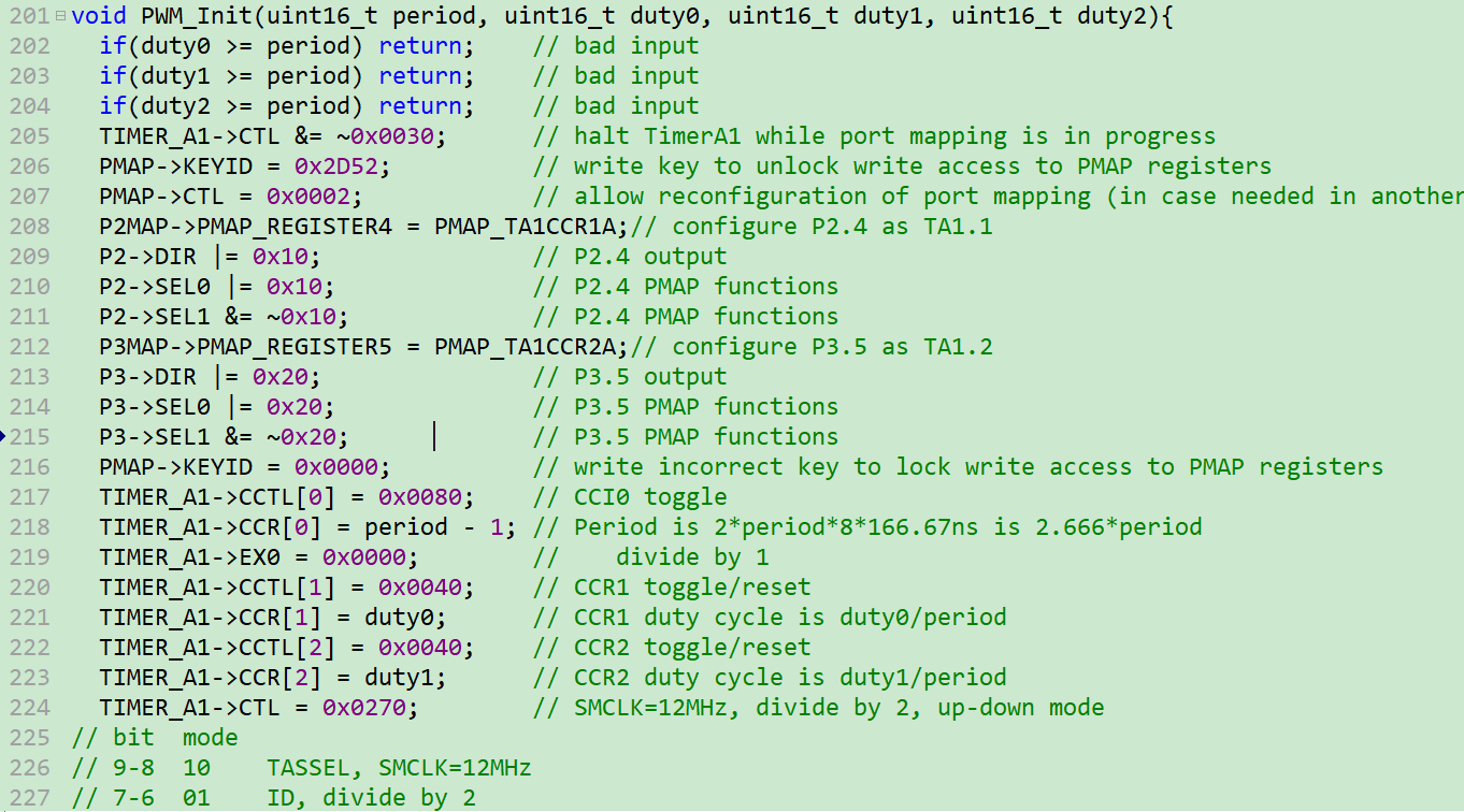
void PWM_Init(uint16_t period, uint16_t duty0, uint16_t duty1, uint16_t duty2){
if(duty0 >= period) return; // bad input
if(duty1 >= period) return; // bad input
if(duty2 >= period) return; // bad input
TIMER_A1->CTL &= ~0x0030; // halt TimerA1 while port mapping is in progress
PMAP->KEYID = 0x2D52; // write key to unlock write access to PMAP registers
PMAP->CTL = 0x0002; // allow reconfiguration of port mapping (in case needed in another module)
P2MAP->PMAP_REGISTER4 = PMAP_TA1CCR1A;// configure P2.4 as TA1.1
P2->DIR |= 0x10; // P2.4 output
P2->SEL0 |= 0x10; // P2.4 PMAP functions
P2->SEL1 &= ~0x10; // P2.4 PMAP functions
P3MAP->PMAP_REGISTER5 = PMAP_TA1CCR2A;// configure P3.5 as TA1.2
P3->DIR |= 0x20; // P3.5 output
P3->SEL0 |= 0x20; // P3.5 PMAP functions
P3->SEL1 &= ~0x20; // P3.5 PMAP functions
PMAP->KEYID = 0x0000; // write incorrect key to lock write access to PMAP registers
TIMER_A1->CCTL[0] = 0x0080; // CCI0 toggle
TIMER_A1->CCR[0] = period - 1; // Period is 2*period*8*166.67ns is 2.666*period
TIMER_A1->EX0 = 0x0000; // divide by 1
TIMER_A1->CCTL[1] = 0x0040; // CCR1 toggle/reset
TIMER_A1->CCR[1] = duty0; // CCR1 duty cycle is duty0/period
TIMER_A1->CCTL[2] = 0x0040; // CCR2 toggle/reset
TIMER_A1->CCR[2] = duty1; // CCR2 duty cycle is duty1/period
TIMER_A1->CTL = 0x0270; // SMCLK=12MHz, divide by 2, up-down mode
// bit mode
// 9-8 10 TASSEL, SMCLK=12MHz
// 7-6 01 ID, divide by 2
// 5-4 11 MC, up-down mode
// 2 0 TACLR, no clear
// 1 0 TAIE, no interrupt
// 0 TAIFG
P5->DIR |= 0x80; // P5.7 output
P5->SEL0 |= 0x80; // P5.7 TimerA2.2 functions
P5->SEL1 &= ~0x80; // P5.7 TimerA2.2 functions
TIMER_A2->CCTL[0] = 0x0080; // CCI0 toggle
TIMER_A2->CCR[0] = period - 1; // Period is 2*period*8*166.67ns is 2.666*period
TIMER_A2->EX0 = 0x0000; // divide by 1
TIMER_A2->CCTL[2] = 0x0040; // CCR2 toggle/reset
TIMER_A2->CCR[2] = duty2; // CCR2 duty cycle is duty2/period
TIMER_A2->CTL = 0x0270; // SMCLK=12MHz, divide by 2, up-down mode
// bit mode
// 9-8 10 TASSEL, SMCLK=12MHz
// 7-6 01 ID, divide by 2
// 5-4 11 MC, up-down mode
// 2 0 TACLR, no clear
// 1 0 TAIE, no interrupt
// 0 TAIFG
}
//***************************PWM_Duty0*******************************
// change duty cycle of PWM output on P2.4
// Inputs: duty0
// Outputs: none
// Period of P2.4 is period*333.33ns, duty cycle is duty0/period
void PWM_Duty0(uint16_t duty0){
if(duty0 >= TIMER_A1->CCR[0]) return; // bad input
TIMER_A1->CCR[1] = duty0; // CCR1 duty cycle is duty0/period
}
//***************************PWM_Duty1*******************************
// change duty cycle of PWM output on P3.5
// Inputs: duty1
// Outputs: none
// Period of P3.5 is period*333.33ns, duty cycle is duty1/period
void PWM_Duty1(uint16_t duty1){
if(duty1 >= TIMER_A1->CCR[0]) return; // bad input
TIMER_A1->CCR[2] = duty1; // CCR2 duty cycle is duty1/period
}
//***************************PWM_Duty2*******************************
// change duty cycle of PWM output on P5.7
// Inputs: duty2
// Outputs: none
// Period of P5.7 is period*333.33ns, duty cycle is duty2/period
void PWM_Duty2(uint16_t duty2){
if(duty2 >= TIMER_A2->CCR[0]) return; // bad input
TIMER_A2->CCR[2] = duty2; // CCR2 duty cycle is duty2/period
}
// end of PWM.c slight modifications
#define HEIGHTARRAYLEN 10
// The full range of the arm height servo should be from 1000 �s (fully raised) to 1900 �s (fully lowered).
const uint16_t HEIGHTDUTY[HEIGHTARRAYLEN] = {3000, 3270, 3540, 3810, 4080, 4350, 4620, 4890, 5160, 5700};
int HeightIndex = 0;
#define TILTARRAYLEN 10
// The full range of the arm tilt servo should be from 1200 �s (fully down) to 1900 �s (fully up).
const uint16_t TILTDUTY[TILTARRAYLEN] = {3600, 3810, 4020, 4230, 4440, 4650, 4860, 5070, 5280, 5700};
int TiltIndex = 0;
#define GRIPARRAYLEN 10
// The full range of the gripper servo should be from about 500 �s (fully open) to 2400 �s (fully closed).
const uint16_t GRIPDUTY[GRIPARRAYLEN] = {1500, 2070, 2640, 3210, 3780, 4350, 4920, 5490, 6060, 7200};
int GripIndex = 0;
void SysTick_Handler(void){ // every 100ms
static uint8_t previous = 0; // previous button status
uint8_t current; // current button status
uint32_t heightADC, tiltADC, gripADC, expectedADC;
P8->OUT ^= 0x80; // toggle P8.7
current = Bump_Read();
if(((current&0x01) == 0x01) && ((previous&0x01) != 0x01)){
if(HeightIndex > 0){
HeightIndex = HeightIndex - 1;
PWM_Duty0(HEIGHTDUTY[HeightIndex]);
}
}
if(((current&0x02) == 0x02) && ((previous&0x02) != 0x02)){
if(HeightIndex < (HEIGHTARRAYLEN - 1)){
HeightIndex = HeightIndex + 1;
PWM_Duty0(HEIGHTDUTY[HeightIndex]);
}
}
if(((current&0x04) == 0x04) && ((previous&0x04) != 0x04)){
if(TiltIndex > 0){
TiltIndex = TiltIndex - 1;
PWM_Duty1(TILTDUTY[TiltIndex]);
}
}
if(((current&0x08) == 0x08) && ((previous&0x08) != 0x08)){
if(TiltIndex < (TILTARRAYLEN - 1)){
TiltIndex = TiltIndex + 1;
PWM_Duty1(TILTDUTY[TiltIndex]);
}
}
if(((current&0x10) == 0x10) && ((previous&0x10) != 0x10)){
if(GripIndex > 0){
GripIndex = GripIndex - 1;
PWM_Duty2(GRIPDUTY[GripIndex]);
}
}
if(((current&0x20) == 0x20) && ((previous&0x20) != 0x20)){
if(GripIndex < (GRIPARRAYLEN - 1)){
GripIndex = GripIndex + 1;
PWM_Duty2(GRIPDUTY[GripIndex]);
}
}
previous = current;
ADC_In21_22_23(&heightADC, &tiltADC, &gripADC);// sample ADC
// Expect an approximately 1:1 correspondence between the servo position in milliseconds and the feedback voltage in millivolts.
// So for example, the feedback voltage will be around 1.5 V at the position corresponding to 1.5 ms servo pulses.
// Convert units of period duration to ADC units:
// (16,384 ADC counts/3.3 V) * (1 V/1 millisecond) * (1 millisecond/3,000 timer counts) =
// (16,384 ADC counts/9,900 timer counts) =
// 1.654949495 ADC counts/timer counts
expectedADC = (HEIGHTDUTY[HeightIndex]<<14)/9900;
if((heightADC > ((expectedADC*110)/100)) || (heightADC < ((expectedADC*90)/100))){
P8->OUT |= 0x01; // turn on P8.0
}else{
P8->OUT &= ~0x01; // turn off P8.0
}
expectedADC = (TILTDUTY[TiltIndex]<<14)/9900;
if((tiltADC > ((expectedADC*110)/100)) || (tiltADC < ((expectedADC*90)/100))){
P8->OUT |= 0x20; // turn on P8.5
}else{
P8->OUT &= ~0x20; // turn off P8.5
}
expectedADC = (GRIPDUTY[GripIndex]<<14)/9900;
if((gripADC > ((expectedADC*110)/100)) || (gripADC < ((expectedADC*90)/100))){
P8->OUT |= 0x40; // turn on P8.6
}else{
P8->OUT &= ~0x40; // turn off P8.6
}
}
void main(void){
DisableInterrupts();
Clock_Init48MHz(); // set system clock to 48 MHz
ADC0_InitSWTriggerCh21_22_23();// initialize channels 21,22,23
PWM_Init(60000, HEIGHTDUTY[0], TILTDUTY[0], GRIPDUTY[0]);
Bump_Init();
P8->SEL0 &= ~0xE1;
P8->SEL1 &= ~0xE1; // configure P8.7-P8.5 and P8.0 as GPIO
P8->DIR |= 0xE1; // make P8.7-P8.5 and P8.0 out
P8->OUT &= ~0xE1; // P8.7-P8.5 and P8.0 initially off
SysTick_Init(4800000, 3); // set up SysTick for 10 Hz interrupts
EnableInterrupts(); // SysTick is priority 3
while(1){
WaitForInterrupt();
}
}
这个您可以看一下数据手册
http://www.ti.com/cn/lit/ds/symlink/msp432p401r.pdf
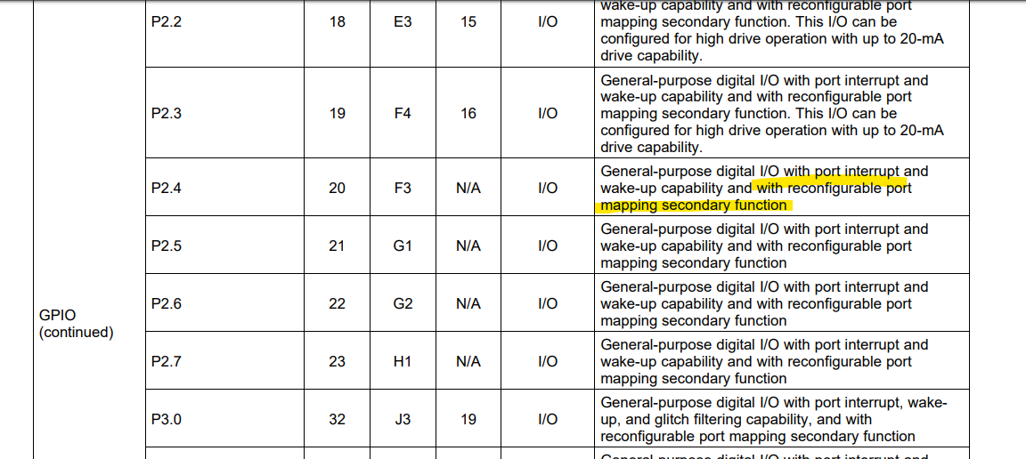
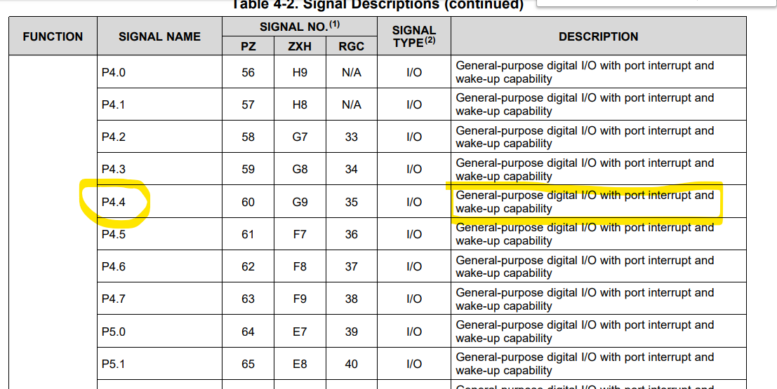
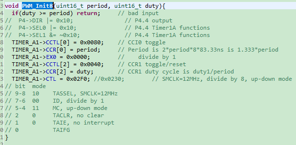
P4.4是不具备reconfigurable port mapping secondary function 这个功能的,也就是说是不可以进行重新配置port map的
如下图所示
建议您选用其他可以重新配置port map的引脚