使用MSP430F6736,想使用LPM3.5模式,官网上例程无LPM3.5的相关配置,是否相关例程呢?如何进入。以及使用LPM3.5模式下与LPM3模式有无特别需要注意的。
This thread has been locked.
If you have a related question, please click the "Ask a related question" button in the top right corner. The newly created question will be automatically linked to this question.
使用MSP430F6736,想使用LPM3.5模式,官网上例程无LPM3.5的相关配置,是否相关例程呢?如何进入。以及使用LPM3.5模式下与LPM3模式有无特别需要注意的。
参考下其他型号的例程
//******************************************************************************
//   MSP430F665x Demo - LPM4.5, Backup RAM
//
//   Description: Board is setup to first init all ports, setup for P1.4 lo/hi
//         transition interrupt, and start XT1 for setting BAKMEM registers.
//         After registers are written, XT1 is disabled, and LPM4.5 is entered.
//         Upon a lo/hi transition to P1.4, the device will awaken from LPM4.5
//         and attempt to verify if the contents remain as they were programmed
//         previous to entering LPM4.5. If so, the LED is lit, if not, the LED
//         will blink quickly. If the device was not properly put into LPM4.5
//         (see NOTE) before the transition was made, the LED will blink slowly
//  NOTE: A backup supply is not required since backup is disabled by setting
//        the BAKDIS bit.
//
//
//   NOTE: This code example was tested on the MSP-TS430PZ100USB Rev1.2 board.
//         To get proper execution of this code example, first switch the JP3
//         to external power, and force 3.0V on the VCC pin. Remove JP1 and set
//         a multimeter on current reading to ensure proper entrance/exit of
//         LPM4.5. Now build the code example and program the device via the
//         Debug button. Press "Run" then "Terminate All" buttons. Detatch the
//         JTAG interface with the FET from the board. You should read around
//         0.38uA current through JP1. Attatch a jumper wire from P1.4 (Pin 38)
//         to Vcc, to trigger a lo/hi transition. The LED on the board should
//         light up, signifying a successful verificaiton of the programmed
//         values for all four BAKMEM registers.
//
//  MCLK = SMCLK = default DCO~1MHz
//
//                MSP430F665x
//             -----------------
//         /|\|                 |
//          | |                 |
//          --|RST              |
//      /|\   |                 |
//       --o--|P1.4         P1.0|-->LED
//      \|/
//
//   P. Thanigai
//   Texas Instruments Inc.
//   May 2012
//   Built with IAR Embedded Workbench Version: 5.40 & CCS V5.2
//******************************************************************************
#include <msp430.h>

void Board_Init(void);
void EnterLPM45(void);
void WakeUpLPM45(void);
void SetBAKMEM(void);

int main(void)
{
  WDTCTL = WDTPW + WDTHOLD;                 // Stop WDT

  if(SYSRSTIV == 0x08)
  {
    WakeUpLPM45();
    P1DIR |= BIT0;                          // P1.0 Output
    // read backup RAM. if values match, turn on LED. else, clear LED.
    if((BAKMEM0==0x0000)&&(BAKMEM1==0x1111)&&(BAKMEM2==0x2222)&&(BAKMEM3==0x3333))
    {
      while(1)
        P1OUT |= BIT0;                      // all values match, turn on LED
    }
    else
    {
      while(1)                              // Blink LED fast if values don't
      {                                     // all match
        P1OUT ^= BIT0;
        __delay_cycles(20000);
      }
    }
  }

  Board_Init();
  SetBAKMEM();
  EnterLPM45();

  P1DIR |= BIT0;                            // Code should NOT go here
  while(1)                                  // Blink LED slow if not an LPM4.5
  {                                         // Wakeup condition
    P1OUT ^= BIT0;
    __delay_cycles(500000);
  }

}

#if defined(__TI_COMPILER_VERSION__) || defined(__IAR_SYSTEMS_ICC__)
#pragma vector=PORT1_VECTOR
__interrupt void Port1_ISR (void)
#elif defined(__GNUC__)
void __attribute__ ((interrupt(PORT1_VECTOR))) Port1_ISR (void)
#else
#error Compiler not supported!
#endif
{
  PMMCTL0_H = PMMPW_H;                      // open PMM
  PM5CTL0 &= ~LOCKIO;                       // Clear LOCKBAK and enable ports
  PMMCTL0_H = 0x00;                         // close PMM

  P1IFG &= ~BIT4;                           // Clear P1.4 IFG
  __bic_SR_register_on_exit(LPM4_bits);     // Exit LPM4.5
  __no_operation();
}

void Board_Init(void)
{
  // Port Configuration
  P1OUT = 0x00;P2OUT = 0x00;P3OUT = 0x00;P4OUT = 0x00;P5OUT = 0x00;P6OUT = 0x00;
  P7OUT = 0x00;P8OUT = 0x00;P9OUT = 0x00;PJOUT = 0x00;
  P1DIR = 0xFF;P2DIR = 0xFF;P3DIR = 0xFF;P4DIR = 0xFF;P5DIR = 0xFF;P6DIR = 0xFF;
  P7DIR = 0xFF;P8DIR = 0xFF;P9DIR = 0xFF;PJDIR = 0xFF;

  // P1.4 Interrupt Configuration
  P1IES &= ~BIT4;                           // P1.4 Lo/Hi edge
  P1IE = BIT4;                              // P1.4 interrupt enabled
  P1IFG = 0;                           		// P1.4 IFG cleared

  // Disable VUSB LDO and SLDO
  USBKEYPID   =     0x9628;                 // set USB KEYandPID to 0x9628
                                            // enable access to USB config reg
  USBPWRCTL &= ~(SLDOEN+VUSBEN);            // Disable the VUSB LDO and the SLDO
  USBKEYPID   =    0x9600;                  // disable access to USB config reg
  __delay_cycles(10000);                    // settle FLL
}

void EnterLPM45(void)
{
  __enable_interrupt();
  // Turn off Clock for LPM4.5 operation
  UCSCTL6 |= XT1OFF;                        // XT1 Off
  BAKCTL |= BAKDIS;                         // Supply power from Vcc, Vbat disabled
  PMMCTL0_H = PMMPW_H;                      // Open PMM Registers for write and set
  PMMCTL0_L |= PMMREGOFF;                   // PMMREGOFF
  __bis_SR_register(LPM4_bits);             // Enter LPM4.5 mode with interrupts
  __no_operation();                         // enabled
}

void WakeUpLPM45(void)
{
  PMMCTL0_H = PMMPW_H;                      // open PMM
  PM5CTL0 &= ~LOCKIO;                       // Clear LOCKIO and enable ports
  PMMCTL0_H = 0x00;                         // close PMM

  // Restore Port settings
  P1OUT = 0x00;P2OUT = 0x00;P3OUT = 0x00;P4OUT = 0x00;P5OUT = 0x00;P6OUT = 0x00;
  P7OUT = 0x00;P8OUT = 0x00;P9OUT = 0x00;PJOUT = 0x00;
  P1DIR = 0xFF;P2DIR = 0xFF;P3DIR = 0xFF;P4DIR = 0xFF;P5DIR = 0xFF;P6DIR = 0xFF;
  P7DIR = 0xFF;P8DIR = 0xFF;P9DIR = 0xFF;PJDIR = 0xFF;

  while(BAKCTL & LOCKBAK)                   // Unlock backup sub system
     BAKCTL &= ~(LOCKBAK);
}

void SetBAKMEM(void)
{
  // Set backup RAM values
  BAKMEM0 = 0x0000;
  BAKMEM1 = 0x1111;
  BAKMEM2 = 0x2222;
  BAKMEM3 = 0x3333;

}
//******************************************************************************
//   MSP430F66x Demo - RTC_B, LPM3.5, & alarm
//
//   Description: The RTC_B module is used to set the time, start RTC operation,
//   and read the time from the respective RTC registers. Software will set the
//   original time to 11:59:45 am on Friday June 22,2012. Then the RTC will
//   be activated through software, and an alarm will be created for the next
//   minute (12:00:00 pm). The device will then enter LPM3.5 awaiting
//   the event interrupt. Upon being woken up by the event, the LED on the board
//   will be set.
//
//   NOTE: This code example was created and tested using the MSP-TS430PZ100USB
//   Rev1.2 board. To ensure that LPM3.5 is entered properly, upon opening the
//   debug window either hit the "Run Free" button on the dropdown menu next to
//   the run button if you are using CCS, or make sure to check that the
//   "Release JTAG on GO" option is selected if you are using IAR.
//   Also ensure Vcc is tied to Vbat if no backup supply is used
//
//  //* An external watch crystal on XIN XOUT is required for ACLK *//
//   ACLK = 32.768kHz, MCLK = SMCLK = default DCO~1MHz
//
//                MSP430F66xx
//             -----------------
//         /|\|              XIN|-
//          | |                 | 32kHz
//          --|RST          XOUT|-
//            |                 |
//            |             P1.0|--> LED
//            |            Vbat |---
//            |                 |  |
//            |            Vcc  |---
//   P. Thanigai
//   Texas Instruments Inc.
//   May 2012
//   Built with IAR Embedded Workbench Version: 5.40 & CCS V5.2
//*****************************************************************************
#include <msp430.h>

void Board_Init(void);
void RTC_Init(void);
void EnterLPM35(void);
void WakeUpLPM35(void);

int main(void)
{
  WDTCTL = WDTPW + WDTHOLD;                 // Stop WDT
  if(SYSRSTIV == 0x08)
  {
    // When woken up from LPM3.5, reinit
    WakeUpLPM35();
    // If woken up at noon, set LED
    if((RTCHOUR == 0x12)&&(RTCMIN == 0x00)&&(RTCSEC == 0x00))
    {
      P1OUT |= BIT0;
      P1DIR |= BIT0;
      while(1);
    }
    // If values do not match, blink LED fast
    else
    {
      while(1)                                  // continuous loop
      {
        P1OUT ^= BIT0;                          // XOR P1.0
        __delay_cycles(20000);                  // Delay
      }
    }
  }

  // Init board & RTC, then enter LPM3.5
  Board_Init();
  RTC_Init();
  EnterLPM35();

  // Code should not get here
  // Blink LED slowly if LPM3.5 not entered properly
  WakeUpLPM35();
  while(1)
  {
    P1OUT ^= BIT0;                          // XOR P1.0
    __delay_cycles(200000);                 // Delay
  }
}

#if defined(__TI_COMPILER_VERSION__) || defined(__IAR_SYSTEMS_ICC__)
#pragma vector=RTC_VECTOR
__interrupt void RTCISR (void)
#elif defined(__GNUC__)
void __attribute__ ((interrupt(RTC_VECTOR))) RTCISR (void)
#else
#error Compiler not supported!
#endif
{
  PMMCTL0_H = PMMPW_H;                      // open PMM
  PM5CTL0 &= ~LOCKIO;                       // Clear LOCKBAK and enable ports
  PMMCTL0_H = 0x00;                         // close PMM

  RTCCTL0 &= ~RTCTEVIFG;
  __bic_SR_register_on_exit(LPM4_bits);     // Exit LPM4.5
  __no_operation();
}

void Board_Init(void)
{
  // Port Configuration
  P1OUT = 0x00;P2OUT = 0x00;P3OUT = 0x00;P4OUT = 0x00;P5OUT = 0x00;P6OUT = 0x00;
  P7OUT = 0x00;P8OUT = 0x00;P9OUT = 0x00;PJOUT = 0x00;
  P1DIR = 0xFF;P2DIR = 0xFF;P3DIR = 0xFF;P4DIR = 0xFF;P5DIR = 0xFF;P6DIR = 0xFF;
  P7DIR = 0xFF;P8DIR = 0xFF;P9DIR = 0xFF;PJDIR = 0xFF;

  // Disable VUSB LDO and SLDO
  USBKEYPID   =     0x9628;                 // set USB KEYandPID to 0x9628
                                            // enable access to USB config reg
  USBPWRCTL &= ~(SLDOEN+VUSBEN);            // Disable the VUSB LDO and the SLDO
  USBKEYPID   =    0x9600;                  // disable access to USB config reg
  __delay_cycles(10000);                    // settle FLL
}

void RTC_Init(void)
{
  // Setup Clock
  UCSCTL6 &= ~(XT1OFF);                     // XT1 On
  UCSCTL6 |= XCAP_3;                        // Internal load cap
  while(BAKCTL & LOCKBAK)                   // Unlock XT1 pins for operation
     BAKCTL &= ~(LOCKBAK);
  do
  {
    UCSCTL7 &= ~(XT2OFFG + XT1LFOFFG + DCOFFG);
                                            // Clear XT2,XT1,DCO fault flags
    SFRIFG1 &= ~OFIFG;                      // Clear fault flags
  }while (SFRIFG1&OFIFG);                   // Test oscillator fault flag

  // Configure RTC_B
  RTCCTL01 |= RTCTEVIE + RTCBCD + RTCHOLD;  // BCD mode, RTC hold, enable RTC
                                            // event interrupt
  RTCYEAR = 0x2012;                         // Year = 0x2012
  RTCMON = 0x06;                            // Month = 0x06 = June
  RTCDAY = 0x22;                            // Day = 0x22 = 22nd
  RTCDOW = 0x05;                            // Day of week = 0x05 = Friday
  RTCHOUR = 0x11;                           // Hour = 0x11
  RTCMIN = 0x59;                            // Minute = 0x59
  RTCSEC = 0x45;                            // Seconds = 0x45

  RTCCTL1 |= RTCTEV_0;                      // Set RTCTEV for 1 minute alarm
  RTCCTL01 &= ~(RTCHOLD);                   // Start RTC calendar mode

  // Turn off Clock for LPM4.5 operation
  UCSCTL6 |= XT1OFF;                        // XT1 Off
}

void EnterLPM35(void)
{
  __enable_interrupt();
  PMMCTL0_H = PMMPW_H;                      // Open PMM Registers for write
  PMMCTL0_L |= PMMREGOFF;                   // and set PMMREGOFF
  __bis_SR_register(LPM4_bits);             // Enter LPM3.5 mode with interrupts
  __no_operation();                         // enabled
}

void WakeUpLPM35(void)
{
  PMMCTL0_H = PMMPW_H;                       // open PMM
  PM5CTL0 &= ~LOCKIO;                        // Clear LOCKBAK and enable ports
  PMMCTL0_H = 0x00;                          // close PMM

  // Restore Port settings
  P1OUT = 0x00;P2OUT = 0x00;P3OUT = 0x00;P4OUT = 0x00;P5OUT = 0x00;P6OUT = 0x00;
  P7OUT = 0x00;P8OUT = 0x00;P9OUT = 0x00;PJOUT = 0x00;
  P1DIR = 0xFF;P2DIR = 0xFF;P3DIR = 0xFF;P4DIR = 0xFF;P5DIR = 0xFF;P6DIR = 0xFF;
  P7DIR = 0xFF;P8DIR = 0xFF;P9DIR = 0xFF;PJDIR = 0xFF;

  // Restore Clock so that RTC will be read
  UCSCTL6 &= ~(XT1OFF);                     // XT1 On
  UCSCTL6 |= XCAP_3;                        // Internal load cap
  while(BAKCTL & LOCKBAK)                   // Unlock XT1 pins for operation
     BAKCTL &= ~(LOCKBAK);
  do
  {
    UCSCTL7 &= ~(XT2OFFG + XT1LFOFFG + DCOFFG);
                                            // Clear XT2,XT1,DCO fault flags
    SFRIFG1 &= ~OFIFG;                      // Clear fault flags
  }while (SFRIFG1&OFIFG);                   // Test oscillator fault flag

  // Reconfig/start RTC
  RTCCTL01 |= RTCBCD + RTCHOLD;
  RTCCTL01 &= ~RTCHOLD;
}
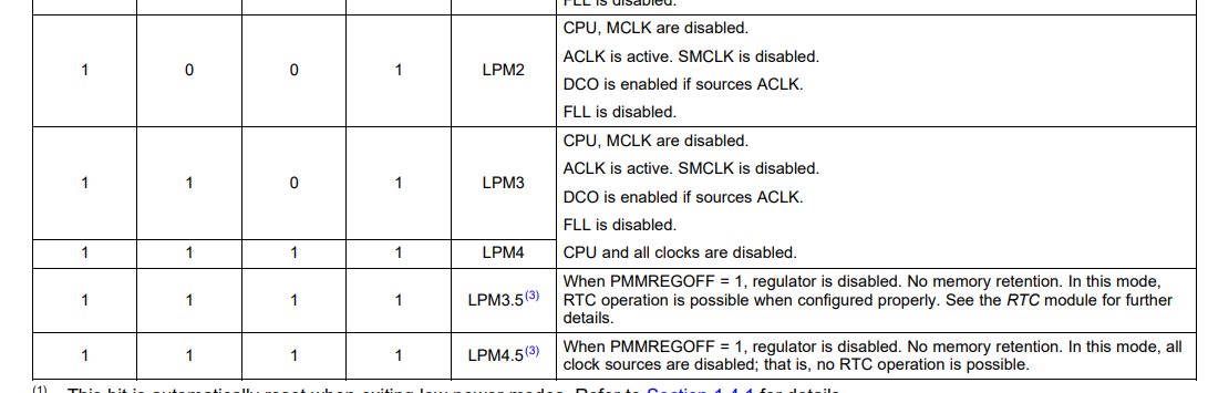
关于LPM3.5 建议您参考下TRM内的内容
http://www.ti.com/lit/ug/slau208q/slau208q.pdf
When LPMx.5 (LPM3.5 or LPM4.5) is entered, the voltage regulator of the Power Management Module(PMM) is disabled. All RAM and register contents are lost. Although the I/O register contents are lost, the I/O pin states are locked upon LPMx.5 entry. See the Digital I/O chapter for further details. Wakeup from LPM4.5 is possible from a power sequence, a RST event, or from specific I/O. Wakeup from LPM3.5 is possible from a power sequence, a RST event, RTC event, or from specific I/O.
以及
1.4.2 Entering and Exiting Low-Power Modes LPMx.5