This thread has been locked.

If you have a related question, please click the "Ask a related question" button in the top right corner. The newly created question will be automatically linked to this question.

MSP430FR6043: Some questions about pulses which is generated on the dedicated CH0_OUT pin

Part Number: MSP430FR6043
Other Parts Discussed in Thread: EVM430-FR6043, MSP430FR6041, MSP430FR5043, MSP430FR5041

Hello!

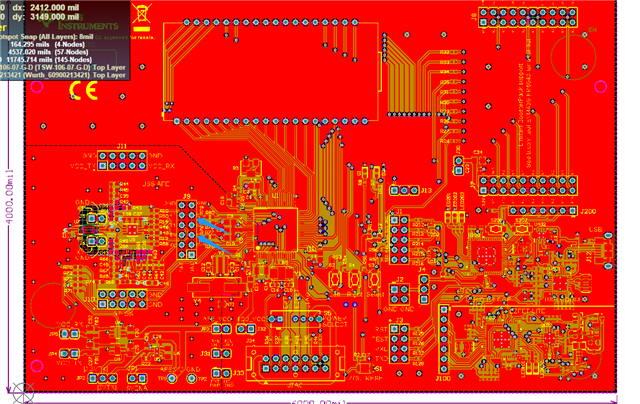
Our company plan to design a water meter using msp430fr6043. We have modified the capacitances and resistances on the EVM430-FR6043 in Figure 1. We used the code examples for msp430fr6043 which named msp430fr6043_saph_01.c, and the code is then posted. We used an oscilloscope to view the waveform of the CH0_OUT pin, as shown in Figure 2,3. The problem we faced was that the oscilloscope waveform was not a square wave, and we suspected that it was not an excitation signal. We want to generate an incentive signal first, but we do not know what is wrong with this, please inform us, thank you very much!
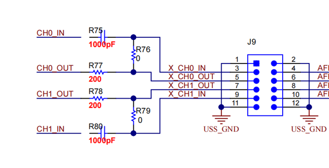
Figure 1
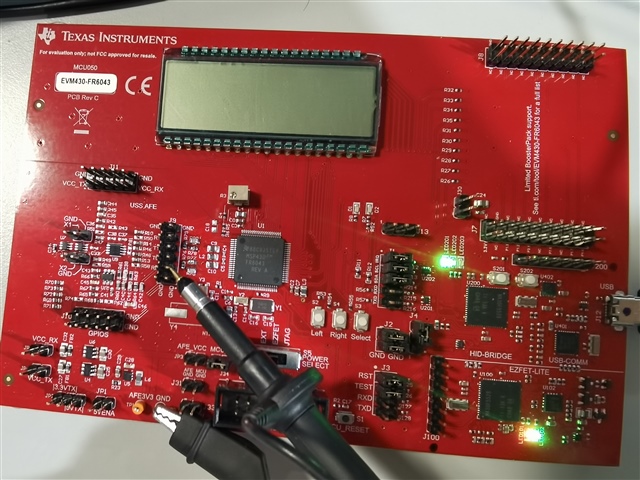
Figure 2
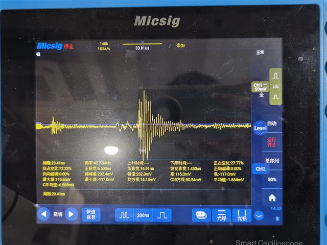
Figure 3

msp430fr6043_saph_01.c

#include <msp430.h>

#define OSCTYPE__CRYSTAL OSCTYPE_0

void HSPLL_init(void);

int main(void)
{
WDTCTL = WDTPW | WDTHOLD; // Stop WDT

// Configure P1.5 as output for LED
P1OUT &= ~BIT5;
P1DIR |= BIT5;

// Disable the GPIO power-on default high-impedance mode to activate
// previously configured port settings
PM5CTL0 &= ~LOCKLPM5;

// Clock System Setup
CSCTL0_H = CSKEY_H; // Unlock CS registers
CSCTL1 = DCOFSEL_3 | DCORSEL; // Set DCO to 8MHz
// Set SMCLK = MCLK = DCO, ACLK = VLOCLK
CSCTL2 = SELA__VLOCLK | SELS__DCOCLK | SELM__DCOCLK;
CSCTL3 = DIVA__1 | DIVS__8 | DIVM__8; // MCLK = SMCLK = 1MHz
CSCTL0_H = 0; // Lock CS registers

HSPLL_init(); // Initialize the HSPLL and wait for it to lock

// Set up the PPG settings
SAPHKEY = KEY; // Unlock the SAPH registers
SAPHPGC = PLEV_0 | PPOL_0 | 0x000A; // 10 excitation pulses, 0 stop pulses, output low when inactive, high polarity
SAPHPGLPER = 40; // Low phase = 40 HSPLL cycles = 500ns
SAPHPGHPER = 40; // High phase = 40 HSPLL cycles = 500ns
SAPHPGCTL = TRSEL_2 | PPGCHSEL_0 | PGSEL_0; // TA2.1 trigger, CH0 output, register mode

// Set up the PHY to output PPG on dedicated CH0_OUT pin
SAPHOSEL = PCH0SEL__PPGSE; // Output PPG

// Enable the PPG
SAPHPGCTL |= PPGEN;

// Configure TA2.1 for ~1/sec to trigger the pulse generation and toggle LED
TA2CCR0 = 9400;
TA2CCR1 = 4700;
TA2CCTL1 = OUTMOD_7 | CCIE; // Enable output signal to trigger PPG, enable Interrupt
TA2CTL = TASSEL__ACLK | TACLR | MC__UP; // Timer sourced from ACLK (VLO), clear timer

while(1)
{
__bis_SR_register(LPM0_bits | GIE); // Enter LPM3 w/interrupt
__no_operation(); // For debug
}
}

// Timer A2 interrupt service routine
#if defined(__TI_COMPILER_VERSION__) || defined(__IAR_SYSTEMS_ICC__)
#pragma vector = TIMER2_A1_VECTOR
__interrupt void Timer2_A1_ISR(void)
#elif defined(__GNUC__)
void __attribute__ ((interrupt(TIMER2_A1_VECTOR))) Timer2_A1_ISR (void)
#else
#error Compiler not supported!
#endif
{
switch(__even_in_range(TA2IV, TAIV__TAIFG))
{
case TAIV__NONE: break; // No interrupt
case TAIV__TACCR1:
P1OUT ^= BIT5; // Toggle LED to show new cycle
break;
case TAIV__TAIFG: break; // overflow
default: break;
}
}

void HSPLL_init(void)
{
// Configure USSXT Oscillator
HSPLLUSSXTLCTL = OSCTYPE__CRYSTAL | USSXTEN;

// Set up timer to wait in LPM for crystal stabilization time = 4096 clocks for crystal resonator.
// For 8MHz XTAL, 4096 clocks = 512us. Using VLO = 9.4kHz, wait 5 timer clock cycles = 532us.
TA4CCR0 = 5;
TA4CCTL0 = CCIE; // Enable Interrupt
TA4CTL = TASSEL__ACLK | TACLR | MC__UP; // Timer sourced from ACLK (VLO), clear timer
__bis_SR_register(LPM3_bits | GIE); // Enter LPM3 w/interrupt
__no_operation(); // For debug

// Check if oscillator is stable
while((HSPLLUSSXTLCTL & OSCSTATE) == 0);

// Output oscillator on pin
HSPLLUSSXTLCTL &= ~XTOUTOFF;

// Init PLL
// Use the PLLM setting to get 80MHz output from our 8MHz input
// Equation: PLL output clock frequency x 2 = input clock frequency x (PLLM+1)
// Input clock frequency = 8MHz
// Desired PLL output clock frequency = 80MHz
// PLLM = 19
HSPLLCTL = PLLM4 | PLLM1 | PLLM0 | PLLINFREQ; //PLLM = 19, PLL input frequency > 6MHz

// Power up the UUPS to start the PLL
UUPSCTL |= USSPWRUP;

// Wait for UUPS to power up
while((UUPSCTL & UPSTATE_3) != UPSTATE_3);

// Wait for PLL to lock
while(!(HSPLLCTL & PLL_LOCK));
}

// Timer A4 interrupt service routine
#if defined(__TI_COMPILER_VERSION__) || defined(__IAR_SYSTEMS_ICC__)
#pragma vector = TIMER4_A0_VECTOR
__interrupt void Timer4_A0_ISR(void)
#elif defined(__GNUC__)
void __attribute__ ((interrupt(TIMER4_A0_VECTOR))) Timer4_A0_ISR (void)
#else
#error Compiler not supported!
#endif
{
// Stop the timer and wake from LPM
TA4CTL = MC__STOP;
__bic_SR_register_on_exit(LPM3_bits | GIE);
__no_operation();
}

  • We have a water meter example code based on FR6043. You can download it from this link. https://www.ti.com/tool/download/USS-SWLIB-WATER

    And there are also app note you can check with. https://www.ti.com/lit/ug/tidues5a/tidues5a.pdf

  • Thank you very much for your reply, but we have read relevant articles and downloaded the code you provided. Since the encapsulation of this code is too high, it is inconvenient to modify the code. So we want to use the examples to send pulses, receive pulses, store data, and calculate the time of flight step by step. So why is my oscilloscope display output pulse not square wave?

  • I have followed these information up.

  • How do you get the oscilloscope figure? Have you attached the transducer on the CHx_OUT pin and then measure the signal?

  • Thank you very much. I found that the parameters of the oscilloscope were wrong, and the waveform in the figure was actually noise. After adjusting the parameters, the oscilloscope could display square waves. But when capturing the waveform, the data was placed in the result array, and I copied the values out. There were only 256. The waveform drawn in excel did not show the receiving pulse. How can I solve this problem?

  • I have followed these information up.

  • It might related to the configuration of the SDHS ADC or the capture sequence. 

    Have you tried with template example first? The ADC capture code is open to the customer in the code. 

  • Yes, the graph is drawn using a template example. The code is as follows. I'm confused about the waveform of the values in the result array. Because I can see waveform on oscilloscope when I captured X_CH0_OUT and X_CH1_IN, as shown in Figure 1 & 2, but not in ccs, as shown in Figure 3. I don't know which step I made a mistake, what should I do?

    Figure 1

    Figure 2

    Figure 3

    //******************************************************************************
    //   MSP430FR60xx Demo - SDHS sampling at 8MSPS and DTC transfer results to RAM
    //
    //   Description: Configure the SDHS for stand-alone use (register mode) at 8MSPS.
    //   Use the DTC to transfer the results to an array in RAM named "results" (located
    //   in LEA RAM at 0x5000). Convert array back to input voltage using:
    //   V = (adc_code * (f_s/2))/(gain*7FF) + Bias
    //   where,adc_code is the ADC result(16-Bit Signed Int),f_s = .755V(Full-scale voltage),
    //   gain = 10^(0.1/20)) = approximately 1, Bias = .9V, 7FF = 2047
    //
    //   ***NOTE: On TS-Board, remove JP14, put SIG on inner pin and GND to outer pin.
    //            Valid input range is 600mV - 1200mV, as configured.***
    //           MSP430FR6043
    //         ---------------
    //     /|\|               |
    //      | |               |
    //      --|RST            |
    //        |           P1.5|---> LED
    //        |               |-USSXTIN
    //        |               |-USSXTOUT
    //        |         CH0_IN|<--- input signal
    //
    //   Gary Gao & Matt Calvo
    //   Texas Instruments Inc.
    //   February 2018
    //   Built with IAR Embedded Workbench V7.10 & Code Composer Studio V7.3
    //******************************************************************************
    #include <msp430.h>
    
    #define OSCTYPE__CRYSTAL OSCTYPE_0
    
    void HSPLL_init(void);
    
    #if defined(__TI_COMPILER_VERSION__)
    #pragma DATA_SECTION(results, ".leaRAM")
    #pragma RETAIN(results)
     int results[800] = {0};
    #elif defined(__IAR_SYSTEMS_ICC__)
    #pragma location=0x5000
    __no_init  int results[800];
    #pragma required = results
    #elif defined(__GNUC__)
     int results[800] __attribute__ ((section (".leaRAM"), used));
    #else
    #error Compiler not supported!
    #endif
    
    int main(void)
    {
    
    
        WDTCTL = WDTPW | WDTHOLD;               // Stop WDT
    
        // Configure P1.5 as output for LED
        P1OUT &= ~BIT5;
        P1DIR |= BIT5;
    
        // Disable the GPIO power-on default high-impedance mode to activate
        // previously configured port settings
        PM5CTL0 &= ~LOCKLPM5;
    
        // Configure one FRAM waitstate as required by the device datasheet for MCLK
        // operation beyond 8MHz _before_ configuring the clock system.
        FRCTL0 = FRCTLPW | NWAITS_1;
    
    
        // Clock System Setup
        CSCTL0_H = CSKEY_H;                     // Unlock CS registers
        // Per Device Errata(CS12) set divider to 4 before changing frequency to
        // prevent out of spec operation from overshoot transient
        CSCTL3 = DIVA__4 | DIVS__4 | DIVM__4;   // Set all corresponding clk sources to divide by 4 for errata(CS12)
        CSCTL1 = DCOFSEL_4 | DCORSEL;           // Set DCO to 16MHz
        // Delay by ~10us to let DCO settle. 60 cycles = 20 cycles buffer + (10us / (1/4MHz))
        __delay_cycles(60);
        CSCTL3 = DIVA__1 | DIVS__1 | DIVM__1;   // Set all dividers to 1 for 16MHz operation
        CSCTL3 = DIVA__1 | DIVS__1 | DIVM__1;   // MCLK = SMCLK = 16MHz
        CSCTL0_H = 0;                           // Lock CS registers


        //Setup SAPH Bias Register Controlled
        SAPHKEY = KEY;
        SAPHBCTL &= ~ASQBSC;                    //Tx bias and Rx bias switches control source select; 0h (R/W) = Bias switches are controlled by SAPHBCTL.CH0EBSW, SAPHBCTL.CH1EBSW, SAPHBCTL.PGABSW bits (register mode)
        SAPHBCTL |= CPDA;                       //Enable the power supply (Charge Pump) for the the input multiplexer during data acquisition. 1h (R/W) = Keep turning on the charge pump during data acquisition.
        SAPHICTL0 = 0;                          //Input Multiplexer Channel Select
        SAPHKEY = KEY+1;
    
    
        //Setup the SDHS with register mode
        SDHSCTL0 = TRGSRC_0 | AUTOSSDIS_1 | DFMSEL_0;// Software trigger,Left, 2s complement format
        SDHSCTL1 = OSR_0;                       // OSR = 10 (80MHz/10 = 8MSPS). CS must set MCLK >= 8MHz.
        SDHSCTL2 = 799;                         // SMPSZ = 255+1 samples
        SDHSCTL6 = 0x20;                        // PGA Gain 0.1 dB
        SDHSCTL7 = 0xC;                         // MODOPTI = 0xC (80MHz PLL output frequency)
        SDHSDTCDA = 0x800;                          // DTC transfer data to start of LEA RAM
        SDHSIMSC = ACQDONE;                     // Enable acquisition done interrupt (after 256 samples transferred)
        SDHSCTL3 = TRIGEN_1;                    // Enable trigger
        SDHSCTL4 = SDHSON;                      // Turn on SD and start conversion
        __delay_cycles(640);                    // Delay for PGA worst case 40us settling time
    
        HSPLL_init();                           // Initialize the HSPLL and wait for it to lock
    
    ///*SAPH
        // Set up the PPG settings
        SAPHKEY = KEY;                          // Unlock the SAPH registers
        SAPHPGC = PLEV_0 | PPOL_0 | 0x000A;     // 10 excitation pulses, 0 stop pulses, output low when inactive, high polarity
        SAPHPGLPER = 40;                         // Low phase = 40 HSPLL cycles = 500ns
        SAPHPGHPER = 40;                         // High phase = 40 HSPLL cycles = 500ns
        SAPHPGCTL = TRSEL_2 | PPGCHSEL_0 | PGSEL_0; // TA2.1 trigger, CH0 output, register mode
    
        // Set up the PHY to output PPG on dedicated CH0_OUT pin
        SAPHOSEL = PCH0SEL__PPGSE;              // Output PPG
    
        // Enable the PPG
        SAPHPGCTL |= PPGEN;
    //SAPH*/
    
        // Configure TA2.1 for 1/sec to trigger the pulse generation and toggle LED
        TA2CCR0 = 9400;
        TA2CCR1 = 4700;
        TA2CCTL1 = OUTMOD_7 | CCIE;             // Enable output signal to trigger PPG, enable Interrupt
        TA2CTL = TASSEL__ACLK | TACLR | MC__UP; // Timer sourced from ACLK (VLO), clear timer
    
        while(1)
        {
            __bis_SR_register(LPM0_bits | GIE); // Enter LPM0 w/interrupt
            __no_operation();                   // For debug
        }
    }
    
    // Timer A2 interrupt service routine
    #if defined(__TI_COMPILER_VERSION__) || defined(__IAR_SYSTEMS_ICC__)
    #pragma vector = TIMER2_A1_VECTOR
    __interrupt void Timer2_A1_ISR(void)
    #elif defined(__GNUC__)
    void __attribute__ ((interrupt(TIMER2_A1_VECTOR))) Timer2_A1_ISR (void)
    #else
    #error Compiler not supported!
    #endif
    {
    
        switch(__even_in_range(TA2IV, TAIV__TAIFG))
        {
    
            case TAIV__NONE:   break;           // No interrupt
            case TAIV__TACCR1:
                SDHSCTL4&= ~SDHSON;
                SDHSCTL5 &= ~SSTART;
                SDHSCTL3 = 0;
                SDHSDTCDA = 0x800;
                SDHSCTL3 = TRIGEN_1;
                SDHSCTL4 = SDHSON;
                SDHSCTL5 |= SSTART;             // Start conversion
                __no_operation();
                break;
            case TAIV__TAIFG:                   // overflow
                __no_operation();
                break;
            default: break;
        }
    }
    
    // SDHS interrupt service routine
    #if defined(__TI_COMPILER_VERSION__) || defined(__IAR_SYSTEMS_ICC__)
    #pragma vector = SDHS_VECTOR
    __interrupt void SDHS_ISR(void)
    #elif defined(__GNUC__)
    void __attribute__ ((interrupt(SDHS_VECTOR))) SDHS_ISR (void)
    #else
    #error Compiler not supported!
    #endif
    {
    
        switch(__even_in_range(SDHSIIDX, IIDX_6))
        {
            case IIDX_0:   break;               // No interrupt
            case IIDX_1:
                __no_operation();
                break;                          // OVF interrupt
            case IIDX_2:                        // ACQDONE interrupt
                P1OUT ^= BIT5;                  // Toggle LED to show new cyclelll
                __delay_cycles(1000);
                __no_operation();               // Put breakpoint here to view results
                break;
            case IIDX_3:   break;               // SSTRG interrupt
            case IIDX_4:   break;               // DTRDY interrupt
            case IIDX_5:   break;               // WINHI interrupt
            case IIDX_6:   break;               // WINLO interrupt
            default: break;
        }
    }
    
    void HSPLL_init(void)
    {
        // Configure USSXT Oscillator
        HSPLLUSSXTLCTL = OSCTYPE__CRYSTAL |  USSXTEN;
    
        // Set up timer to wait in LPM for crystal stabilization time = 4096 clocks for crystal resonator.
        // For 8MHz XTAL, 4096 clocks = 512us. Using VLO = 9.4kHz, wait 5 timer clock cycles = 532us.
        TA4CCR0 = 5;
        TA4CCTL0 = CCIE;                        // Enable Interrupt
        TA4CTL = TASSEL__ACLK | TACLR | MC__UP; // Timer sourced from ACLK (VLO), clear timer
        __bis_SR_register(LPM3_bits | GIE);     // Enter LPM3 w/interrupt
        __no_operation();                       // For debug
    
        // Check if oscillator is stable
        while((HSPLLUSSXTLCTL & OSCSTATE) == 0);
    
        // Output oscillator on pin
        HSPLLUSSXTLCTL &= ~XTOUTOFF;
    
        // Init PLL
        // Use the PLLM setting to get 80MHz output from our 8MHz input
        // Equation: PLL output clock frequency x 2 = input clock frequency x (PLLM+1)
        // Input clock frequency = 8MHz
        // Desired PLL output clock frequency = 80MHz
        // PLLM = 19
        HSPLLCTL = PLLM4 | PLLM1 | PLLM0 | PLLINFREQ; //PLLM = 19, PLL input frequency > 6MHz
    
        // Power up the UUPS to start the PLL
        UUPSCTL |= USSPWRUP;
    
        // Wait for UUPS to power up
        while((UUPSCTL & UPSTATE_3) != UPSTATE_3);
    
        // Wait for PLL to lock
        while(!(HSPLLCTL & PLL_LOCK));
    }
    
    // Timer A4 interrupt service routine
    #if defined(__TI_COMPILER_VERSION__) || defined(__IAR_SYSTEMS_ICC__)
    #pragma vector = TIMER4_A0_VECTOR
    __interrupt void Timer4_A0_ISR(void)
    #elif defined(__GNUC__)
    void __attribute__ ((interrupt(TIMER4_A0_VECTOR))) Timer4_A0_ISR (void)
    #else
    #error Compiler not supported!
    #endif
    {
        // Stop the timer and wake from LPM
        TA4CTL = MC__STOP;
        __bic_SR_register_on_exit(LPM3_bits | GIE);
        __no_operation();
    }
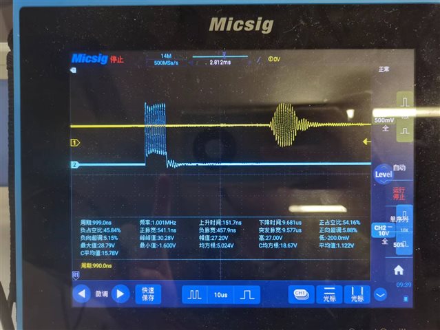
    

  • I have already updated your reply.

  • I saw the answer from the relevant engineer. How to communicate offline?

  • I will discuss with Cash offline, and then get back to you. Thanks for your patience.

  • What‘s the exact demo you use(the code you upload)? Could you please provide me the path?

    And what is the difference you made from the original code?

    According to the waveform, we think the transceivers are working normally.

    but not in ccs, as shown in Figure 3

    So we think that the configurations of ADC in code may be improper.

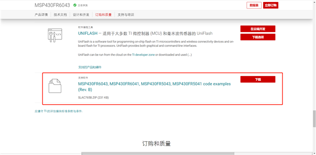
  • Thank you for your answer. I used msp430fr6043_saph_01.c and msp430fr6043_sdhs_01. c in  MSP430FR6043_MSP430FR6041_MSP430FR5043_MSP430FR5041_Code_Examples from the website: https://www.ti.com.cn/product/zh-cn/MSP430FR6043#software-development  .  See Figure 1 for details.

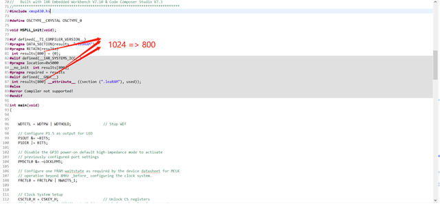
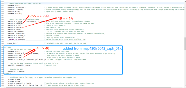
    I added saph excitation in msp430fr6043_sdhs_01.c file and modified the value of array, sampling value and gain. See Figure 2, 3 for details.

    Figure 

    Figure 2

    Figure 3

  • Figure 

    As we mentioned before, this may be the reason why you cannot demonstrate a whole waveform based on the ADC result stored in the device.

    And, the demo in the link you posted is the general demo of these series devices. We have specialized SDK for USS application:

    https://www.ti.com.cn/tool/cn/MSP-ULTRASONIC-DESIGN-CENTER

    It's include the base USS project and a GUI. After you programmed the base project, you can use the GUI to configure the USS parameters, capture the waveform, calculate the relevant result, etc.. It's easy to create your own application and test it.

    The relevant document is in the link and GUI-->help.

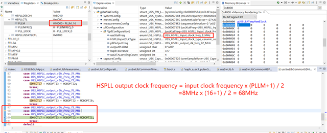
  • Thank you for your answer. I used the GUI and downloaded the corresponding program on the development board. When I read the program, I was a little confused. The "MSP430FR6xx Family User's Guide" file states the formula shown in Figure 1. Combined with the formula and the HSPLLCTL register, the output clock frequency is 68MHz, but the program enters 72Mhz, as shown in Figure 2. Is there any problem with this?

    Figure 1

    Figure 2

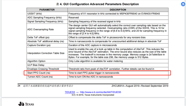
  • Hello, I can't understand the parameter "Start PPG Count", may I ask what time it refers to?

  • What is the basis of parameter selection here? Is it related to hardware circuit? What is the effect of choosing different impedance on the actual measurement? Is it related to the analog to digital conversion offset? Thanks!

  • About the meaning and setting of the parameters, you can reference this page to understand:

    file:///C:/ti/msp/USS_02_30_00_03/USS/docs/UserGuide/UserGuide/ch_config.html

  • Thank you, but I cannot find how to choose the parameters about BIMP in ch_config.html and MSP430FR6xx Family User's Guide. Could you tell me how to make the seletion?

  • Is the interrupt function all written in "USS_Lib_HAL.c"? I configured TA1's interrupt earlier, but why is there no interrupt function about TA1 in "USS_Lib_HAL.c" ?

  • Hi, I strongly suggest you ask a new question for other issues:

    It make us identify and follow up easier. Thanks 

  • Fine. I will close this thread.