If you have a related question, please click the "Ask a related question" button in the top right corner. The newly created question will be automatically linked to this question.
IP 封装箱是对知识产权的保护,290页这段仔细读一下,这段空间只可以这段地址代码访问,外部是访问不到的,不管哪怕是DMA或者JTAG方式,不像Flash存储技术,而铁电是用原子的位置表示0和1,哪怕剖片在电子显微镜下可以无法观察到,换句话说,不管物理方式还是技术方式,都无法破解这段区域,非常有利于对核心知识产权的保护,IP封装箱类似于一个黑盒子,你可以用来存储核心算法或者密钥等
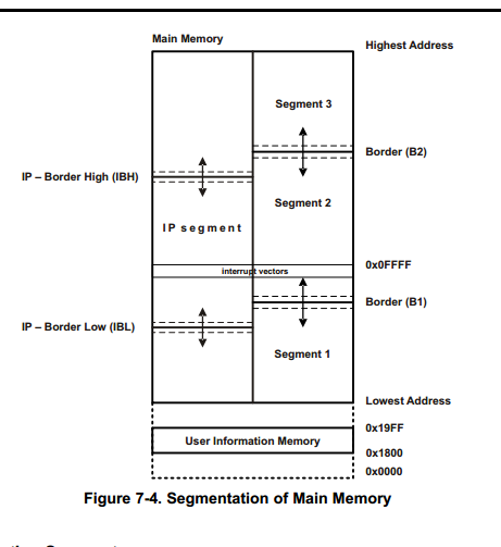
Only program code executed from the IPE segment can access data stored in this segment. The access
rights are evaluated with each code access. Each code access outside of the IP-protected area
deactivates the data access into the IPE segment. JTAG or DMA cannot access the IPE segment. The
interrupt vector table is always open for read and write accesses (for details see Section 7.4.1).
I have corresponded with you at TI-E2E before about this subject.
I am going to get into the details of IPE without either IAR or CCS. What did you get with IAR and CCS? I would like to know your findings.
My initial finding are contradictory to what slau367f.pdf said. But I need to run more test.
I am using a FR6989-LP rev 1.0 and I depend on TIs MSP430Flasher_1.3.3 only. Have you used that before? Do you want to exchange details of what you and I are doing?
I can read Chinese, but it takes too long from me the type anything.
Well, as I dig deeper into that User’s Guide, I found that it is actually more or less correct. And I managed to use NotePad and MSP430Flasher to do IPE.
Here are my answers your questions.
(1) Once the IPE is done (whether by IAE, CCS, or MSP430Flasher), that part of the FRAM cannot be read or written any more (unless you do “ERASE_TOTAL” first). But you still can execute the code inside the IPE. Power cycle, BOR, etc. will not change it. And you do not need the signatures or the data structure any more.
(2) IAR (CCS or MSP430Flasher) can still use that chip the “normal” way. Except they cannot read or write inside the IPE or change its boundaries unless they do “ERASE_TOTAL” first.