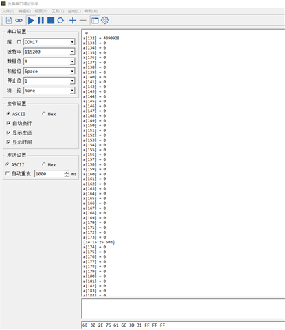
在官方例程adc0_singleended_multichannel_timertrigger_dmareq_MSP_EXP432E401Y 中,如果直接将srcBuffer[0]的值赋给定义的数组,最后得到的数据不是预期的。
代码如下所示,在while循环中直接将srcBuffer的值赋给a[i],得到的结果并不是预期的值。
请问这个是什么原因,同时如果想要将缓冲区的数据读取到指定的数组当中,应该用什么样的方法。
/* --COPYRIGHT--,BSD
 * Copyright (c) 2017, Texas Instruments Incorporated
 * All rights reserved.
 *
 * Redistribution and use in source and binary forms, with or without
 * modification, are permitted provided that the following conditions
 * are met:
 *
 * *  Redistributions of source code must retain the above copyright
 *    notice, this list of conditions and the following disclaimer.
 *
 * *  Redistributions in binary form must reproduce the above copyright
 *    notice, this list of conditions and the following disclaimer in the
 *    documentation and/or other materials provided with the distribution.
 *
 * *  Neither the name of Texas Instruments Incorporated nor the names of
 *    its contributors may be used to endorse or promote products derived
 *    from this software without specific prior written permission.
 *
 * THIS SOFTWARE IS PROVIDED BY THE COPYRIGHT HOLDERS AND CONTRIBUTORS "AS IS"
 * AND ANY EXPRESS OR IMPLIED WARRANTIES, INCLUDING, BUT NOT LIMITED TO,
 * THE IMPLIED WARRANTIES OF MERCHANTABILITY AND FITNESS FOR A PARTICULAR
 * PURPOSE ARE DISCLAIMED. IN NO EVENT SHALL THE COPYRIGHT OWNER OR
 * CONTRIBUTORS BE LIABLE FOR ANY DIRECT, INDIRECT, INCIDENTAL, SPECIAL,
 * EXEMPLARY, OR CONSEQUENTIAL DAMAGES (INCLUDING, BUT NOT LIMITED TO,
 * PROCUREMENT OF SUBSTITUTE GOODS OR SERVICES; LOSS OF USE, DATA, OR PROFITS;
 * OR BUSINESS INTERRUPTION) HOWEVER CAUSED AND ON ANY THEORY OF LIABILITY,
 * WHETHER IN CONTRACT, STRICT LIABILITY, OR TORT (INCLUDING NEGLIGENCE OR
 * OTHERWISE) ARISING IN ANY WAY OUT OF THE USE OF THIS SOFTWARE,
 * EVEN IF ADVISED OF THE POSSIBILITY OF SUCH DAMAGE.
 * --/COPYRIGHT--*/
/******************************************************************************
 * MSP432E4 Example project for ADC with multiple channel and single sequencer
 * with Timer Trigger and DMA Request from ADC.
 *
 * Description: In this application example the ADC0 is configured for a single
 * sequencer sampling 4 channels in single ended mode. The ADC is triggered by
 * a timer running in periodic mode with a sampling frequency of 1 KHz. After
 * the conversion is completed a DMA request is generated by the ADC Sequencer.
 * The data is read by the DMA and an interrupt request to the CPU is
 * generated. The CPU reads the data from the DMA buffer and re-enables the
 * DMA to transfer more data.
 *
 *                MSP432E401Y
 *             ------------------
 *         /|\|               PE3|<-- AIN0
 *          | |               PE2|<-- AIN1
 *          --|RST            PE1|<-- AIN2
 *            |               PE0|<-- AIN3
 *            |                  |
 *            |                  |
 *            |               PA0|<--U0RX
 *            |               PA1|-->U0TX
 * Author: Amit Ashara
*******************************************************************************/
/* DriverLib Includes */
#include <ti/devices/msp432e4/driverlib/driverlib.h>

/* Standard Includes */
#include <stdint.h>
#include <stdbool.h>

/* Display Include via console */
#include "uartstdio.h"

static uint16_t srcBuffer[4];

volatile bool bgetConvStatus = false;;

/* The control table used by the uDMA controller.  This table must be aligned
 * to a 1024 byte boundary. */
#if defined(__ICCARM__)
#pragma data_alignment=1024
uint8_t pui8ControlTable[1024];
#elif defined(__TI_ARM__)
#pragma DATA_ALIGN(pui8ControlTable, 1024)
uint8_t pui8ControlTable[1024];
#else
uint8_t pui8ControlTable[1024] __attribute__ ((aligned(1024)));
#endif


void ADC0SS2_IRQHandler(void)
{
    uint32_t getIntStatus;

    /* Get the interrupt status from the ADC */
    getIntStatus = MAP_ADCIntStatusEx(ADC0_BASE, true);

    /* If the interrupt status for Sequencer-2 is set the
     * clear the status and read the data */
    if((getIntStatus & ADC_INT_DMA_SS2) == ADC_INT_DMA_SS2)
    {
        /* Clear the ADC interrupt flag. */
        MAP_ADCIntClearEx(ADC0_BASE, ADC_INT_DMA_SS2);

        /* Reconfigure the channel control structure and enable the channel */
        MAP_uDMAChannelTransferSet(UDMA_CH16_ADC0_2 | UDMA_PRI_SELECT,
                                   UDMA_MODE_BASIC,
                                   (void *)&ADC0->SSFIFO2, (void *)&srcBuffer,
                                   sizeof(srcBuffer)/2);

        MAP_uDMAChannelEnable(UDMA_CH16_ADC0_2);

        /* Set conversion flag to true */
        bgetConvStatus = true;
    }
}

void ConfigureUART(uint32_t systemClock)
{
    /* Enable the clock to GPIO port A and UART 0 */
    MAP_SysCtlPeripheralEnable(SYSCTL_PERIPH_GPIOA);
    MAP_SysCtlPeripheralEnable(SYSCTL_PERIPH_UART0);

    /* Configure the GPIO Port A for UART 0 */
    MAP_GPIOPinConfigure(GPIO_PA0_U0RX);
    MAP_GPIOPinConfigure(GPIO_PA1_U0TX);
    MAP_GPIOPinTypeUART(GPIO_PORTA_BASE, GPIO_PIN_0 | GPIO_PIN_1);

    /* Configure the UART for 115200 bps 8-N-1 format */
    UARTStdioConfig(0, 115200, systemClock);
}

void swap(int* arr1, int* arr2, int index){
    int j = index;
    int i = 0;
    for(i = 0; i < 256; i++,j++){
        arr2[j] = arr1[i];
    }

}

int main(void)
{
    uint32_t systemClock;

    /* Configure the system clock for 120 MHz */
    systemClock = MAP_SysCtlClockFreqSet((SYSCTL_XTAL_25MHZ | SYSCTL_OSC_MAIN |
                                          SYSCTL_USE_PLL | SYSCTL_CFG_VCO_480),
                                          120000000);

    /* Initialize serial console */
    ConfigureUART(systemClock);

    /* Enable the clock to GPIO Port E and wait for it to be ready */
    MAP_SysCtlPeripheralEnable(SYSCTL_PERIPH_GPIOE);
    while(!(MAP_SysCtlPeripheralReady(SYSCTL_PERIPH_GPIOE)))
    {
    }

    /* Configure PE0-PE3 as ADC input channel */
    MAP_GPIOPinTypeADC(GPIO_PORTE_BASE, GPIO_PIN_3);

    /* Enable the clock to ADC-0 and wait for it to be ready */
    MAP_SysCtlPeripheralEnable(SYSCTL_PERIPH_ADC0);
    while(!(MAP_SysCtlPeripheralReady(SYSCTL_PERIPH_ADC0)))
    {
    }

    /* Configure Sequencer 2 to sample the analog channel : AIN0-AIN3. The
     * end of conversion and interrupt generation is set for AIN3 */
    MAP_ADCSequenceStepConfigure(ADC0_BASE, 2, 0, ADC_CTL_CH1 | ADC_CTL_IE |
                                 ADC_CTL_END);

    /* Enable sample sequence 2 with a timer signal trigger.  Sequencer 2
     * will do a single sample when the timer generates a trigger on timeout*/
    MAP_ADCSequenceConfigure(ADC0_BASE, 2, ADC_TRIGGER_TIMER, 2);

    /* Clear the interrupt status flag before enabling. This is done to make
     * sure the interrupt flag is cleared before we sample. */
    MAP_ADCIntClearEx(ADC0_BASE, ADC_INT_DMA_SS2);
    MAP_ADCIntEnableEx(ADC0_BASE, ADC_INT_DMA_SS2);

    /* Enable the DMA request from ADC0 Sequencer 2 */
    MAP_ADCSequenceDMAEnable(ADC0_BASE, 2);

    /* Since sample sequence 2 is now configured, it must be enabled. */
    MAP_ADCSequenceEnable(ADC0_BASE, 2);

    /* Enable the Interrupt generation from the ADC-0 Sequencer */
    MAP_IntEnable(INT_ADC0SS2);

    /* Enable the DMA and Configure Channel for TIMER0A for Ping Pong mode of
     * transfer */
    MAP_SysCtlPeripheralEnable(SYSCTL_PERIPH_UDMA);
    while(!(SysCtlPeripheralReady(SYSCTL_PERIPH_UDMA)))
    {
    }

    MAP_uDMAEnable();

    /* Point at the control table to use for channel control structures. */
    MAP_uDMAControlBaseSet(pui8ControlTable);

    /* Map the ADC0 Sequencer 2 DMA channel */
    MAP_uDMAChannelAssign(UDMA_CH16_ADC0_2);
    /* Put the attributes in a known state for the uDMA ADC0 Sequencer 2
     * channel. These should already be disabled by default. */
    MAP_uDMAChannelAttributeDisable(UDMA_CH16_ADC0_2,
                                    UDMA_ATTR_ALTSELECT | UDMA_ATTR_USEBURST |
                                    UDMA_ATTR_HIGH_PRIORITY |
                                    UDMA_ATTR_REQMASK);

    /* Configure the control parameters for the primary control structure for
     * the ADC0 Sequencer 2 channel. The primary control structure is used for
     * copying the data from ADC0 Sequencer 2 FIFO to srcBuffer. The transfer
     * data size is 16 bits and the source address is not incremented while
     * the destination address is incremented at 16-bit boundary.
     */
    MAP_uDMAChannelControlSet(UDMA_CH16_ADC0_2 | UDMA_PRI_SELECT,
                              UDMA_SIZE_16 | UDMA_SRC_INC_NONE | UDMA_DST_INC_16 |
                              UDMA_ARB_4);

    /* Set up the transfer parameters for the ADC0 Sequencer 2 primary control
     * structure. The mode is Basic mode so it will run to completion. */
    MAP_uDMAChannelTransferSet(UDMA_CH16_ADC0_2 | UDMA_PRI_SELECT,
                               UDMA_MODE_BASIC,
                               (void *)&ADC0->SSFIFO2, (void *)&srcBuffer,
                               sizeof(srcBuffer)/2);

    /* The uDMA ADC0 Sequencer 2 channel is primed to start a transfer. As
     * soon as the channel is enabled and the Timer will issue an ADC trigger,
     * the ADC will perform the conversion and send a DMA Request. The data
     * transfers will begin. */
    MAP_uDMAChannelEnable(UDMA_CH16_ADC0_2);

    /* Enable Timer-0 clock and configure the timer in periodic mode with
     * a frequency of 1 KHz. Enable the ADC trigger generation from the
     * timer-0. */
    MAP_SysCtlPeripheralEnable(SYSCTL_PERIPH_TIMER0);
    while(!(MAP_SysCtlPeripheralReady(SYSCTL_PERIPH_TIMER0)))
    {
    }

    MAP_TimerConfigure(TIMER0_BASE, TIMER_CFG_A_PERIODIC);
    MAP_TimerLoadSet(TIMER0_BASE, TIMER_A, (systemClock/1000));
    MAP_TimerADCEventSet(TIMER0_BASE, TIMER_ADC_TIMEOUT_A);
    MAP_TimerControlTrigger(TIMER0_BASE, TIMER_A, true);
    MAP_TimerEnable(TIMER0_BASE, TIMER_A);


    int a[256];
    int i=0;
    /* Wait loop */
    while(1){
               /* Wait for the conversion to complete */
                 while(i<256)
                 {
                 a[i]=srcBuffer[0];
                 i++;
                 }
            for(i=0;i<256;i++)
                UARTprintf("a[%d] = %d\r",i, a[i]);
            }
}