This thread has been locked.

If you have a related question, please click the "Ask a related question" button in the top right corner. The newly created question will be automatically linked to this question.

求教Tiva C Launchpad ADC配置问题

uint32_t   Buffer[1];

/*延时1ms*/

void delay_Nms(int n)
{
    int k = 0;
    for(k = n;k > 0;k--)
    SysCtlDelay(SysCtlClockGet() / 3000);
}

void InitADC()
{
   SysCtlPeripheralEnable(SYSCTL_PERIPH_ADC1);

   delay_Nms(1);

    SysCtlPeripheralEnable(SYSCTL_PERIPH_GPIOD);

    delay_Nms(1);

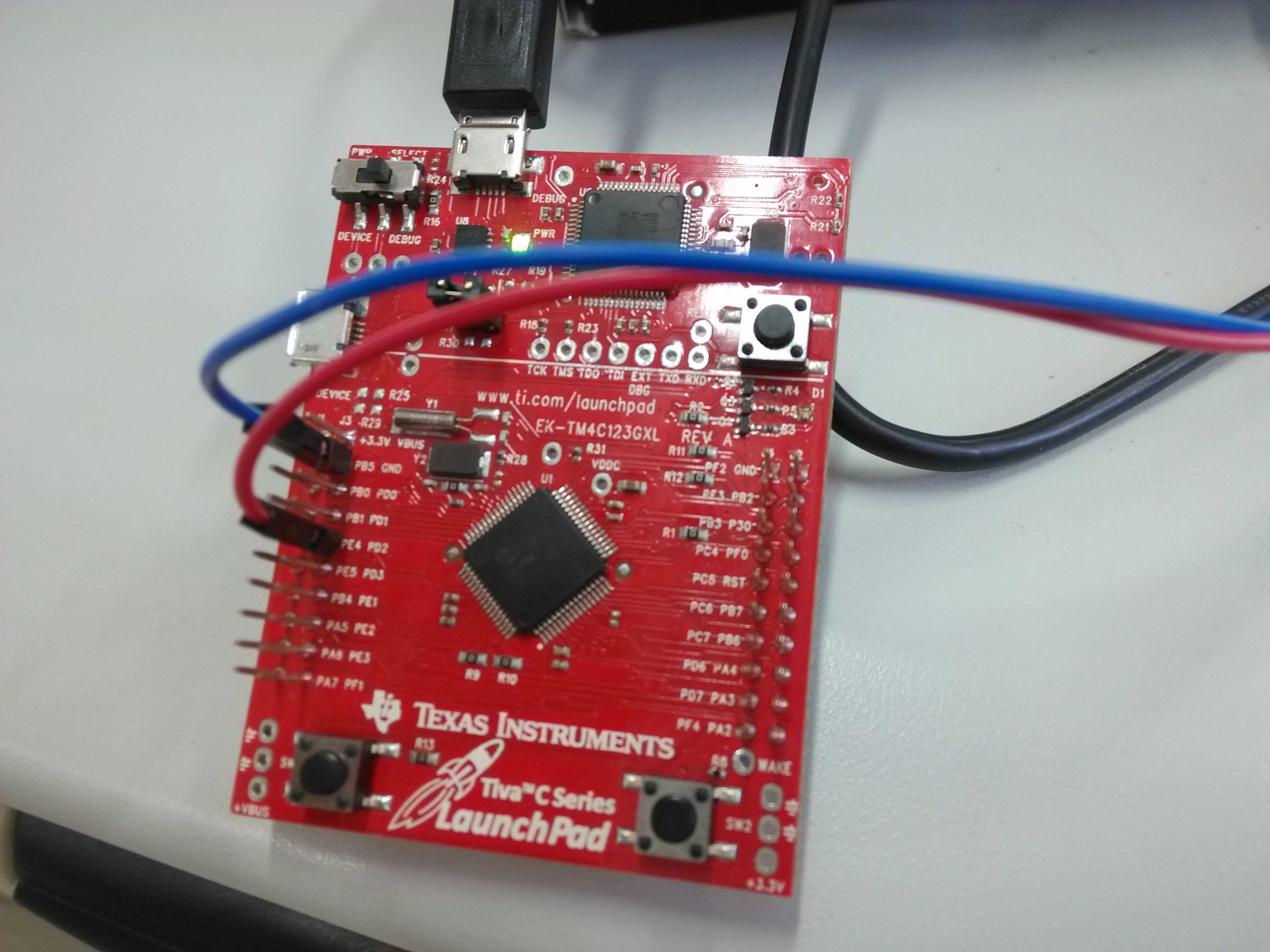
    GPIOPinTypeADC(GPIO_PORTD_BASE,GPIO_PIN_2);

    delay_Nms(1);
    ADCSequenceConfigure(ADC1_BASE, 3, ADC_TRIGGER_PROCESSOR, 0);

    delay_Nms(1);
    ADCSequenceStepConfigure(ADC1_BASE, 3, 0, ADC_CTL_CH0 | ADC_CTL_IE | ADC_CTL_END);

    delay_Nms(1);
    ADCReferenceSet(ADC1_BASE, ADC_REF_INT);

    delay_Nms(1);
    ADCIntEnable(ADC1_BASE,3);

    delay_Nms(1);
    IntEnable(INT_ADC1SS3_TM4C123);

    delay_Nms(1);
    IntMasterEnable();

    delay_Nms(1);
    ADCIntClear(ADC1_BASE,3);

    delay_Nms(1);
    ADCSequenceEnable(ADC1_BASE,3);

    delay_Nms(1);
}

void main(void)

  SysCtlClockSet(SYSCTL_SYSDIV_10    |SYSCTL_USE_PLL        |SYSCTL_OSC_MAIN    | SYSCTL_XTAL_16MHZ);delay_Nms(1);

   InitADC();

   while(1)

   {

        ADCProcessorTrigger(ADC1_BASE, 3);
        while(!ADCIntStatus(ADC1_BASE, 3, false))
        {
        }
        ADCIntClear(ADC1_BASE, 3);
        ADCSequenceUnderflowClear(ADC1_BASE,3);
        ADCSequenceDataGet(ADC1_BASE, 3, Buffer);

    }

}

这样配置后在PD2和GND间加上直流模拟电压,单步调试,却发现无论加不加电压\无论加的电压有何变化,FIFO中读到的值都一直在300(十进制)左右徘徊,

感觉就像是这个待转换的电压完全没有加到ADC上一样,而检测到的看起来像是噪声一样.

于是我在观察列表里查看了Buffer的值和几个寄存器,

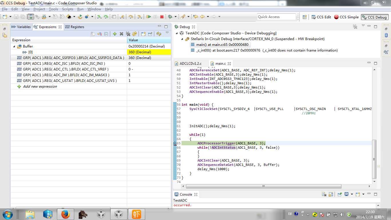
发现从头至尾这个信道的UnderFlow标志和InterruptMask标志都是1,

而且,虽然我设置了Vref为内部的3V参考电压,但是这个ADC_CTL_VREF寄存器也是始终显示的0-....请问这些寄存器的值是说明我配置出错了吗?

新学M4,请多指教,求专家~

  • share一个ADC的例子如下。这里采用的中断方式读取,需要在启动文件中把中断向量表里把中断函数加上即可。

    //*****************************************************************************
    //
    // single_ended.c - Example demonstrating how to configure the ADC for
    // single ended operation.
    //
    // Copyright (c) 2010-2013 Texas Instruments Incorporated. All rights reserved.
    // Software License Agreement
    //
    // Redistribution and use in source and binary forms, with or without
    // modification, are permitted provided that the following conditions
    // are met:
    //
    // Redistributions of source code must retain the above copyright
    // notice, this list of conditions and the following disclaimer.
    //
    // Redistributions in binary form must reproduce the above copyright
    // notice, this list of conditions and the following disclaimer in the
    // documentation and/or other materials provided with the
    // distribution.
    //
    // Neither the name of Texas Instruments Incorporated nor the names of
    // its contributors may be used to endorse or promote products derived
    // from this software without specific prior written permission.
    //
    // THIS SOFTWARE IS PROVIDED BY THE COPYRIGHT HOLDERS AND CONTRIBUTORS
    // "AS IS" AND ANY EXPRESS OR IMPLIED WARRANTIES, INCLUDING, BUT NOT
    // LIMITED TO, THE IMPLIED WARRANTIES OF MERCHANTABILITY AND FITNESS FOR
    // A PARTICULAR PURPOSE ARE DISCLAIMED. IN NO EVENT SHALL THE COPYRIGHT
    // OWNER OR CONTRIBUTORS BE LIABLE FOR ANY DIRECT, INDIRECT, INCIDENTAL,
    // SPECIAL, EXEMPLARY, OR CONSEQUENTIAL DAMAGES (INCLUDING, BUT NOT
    // LIMITED TO, PROCUREMENT OF SUBSTITUTE GOODS OR SERVICES; LOSS OF USE,
    // DATA, OR PROFITS; OR BUSINESS INTERRUPTION) HOWEVER CAUSED AND ON ANY
    // THEORY OF LIABILITY, WHETHER IN CONTRACT, STRICT LIABILITY, OR TORT
    // (INCLUDING NEGLIGENCE OR OTHERWISE) ARISING IN ANY WAY OUT OF THE USE
    // OF THIS SOFTWARE, EVEN IF ADVISED OF THE POSSIBILITY OF SUCH DAMAGE.
    //
    // This is part of revision 1.1 of the Tiva Firmware Development Package.
    //
    //*****************************************************************************

    #include <stdbool.h>
    #include <stdint.h>
    #include "inc/hw_memmap.h"
    #include "driverlib/adc.h"
    #include "driverlib/gpio.h"
    #include "driverlib/pin_map.h"
    #include "driverlib/sysctl.h"
    #include "driverlib/uart.h"
    #include "utils/uartstdio.h"

    #include "driverlib/interrupt.h"

    #include "inc/hw_ints.h"
    #include "inc/hw_types.h"
    #include "inc/hw_adc.h"

    //*****************************************************************************
    //
    //! \addtogroup adc_examples_list
    //! <h1>Single Ended ADC (single_ended)</h1>
    //!
    //! This example shows how to setup ADC0 as a single ended input and take a
    //! single sample on AIN0/PE7.
    //!
    //! This example uses the following peripherals and I/O signals. You must
    //! review these and change as needed for your own board:
    //! - ADC0 peripheral
    //! - GPIO Port E peripheral (for AIN0 pin)
    //! - AIN0 - PE7
    //!
    //! The following UART signals are configured only for displaying console
    //! messages for this example. These are not required for operation of the
    //! ADC.
    //! - UART0 peripheral
    //! - GPIO Port A peripheral (for UART0 pins)
    //! - UART0RX - PA0
    //! - UART0TX - PA1
    //!
    //! This example uses the following interrupt handlers. To use this example
    //! in your own application you must add these interrupt handlers to your
    //! vector table.
    //! - None.
    //
    //*****************************************************************************
    #define ADCSAMPLERATE_1MSPS 0x7 // 1,000,000 samples per second
    #define ADCSAMPLERATE_500KSPS 0x5 // 500,000 samples per second
    #define ADCSAMPLERATE_250KSPS 0x3 // 250,000 samples per second
    #define ADCSAMPLERATE_125KSPS 0x1 // 125,000 samples per second
    //*****************************************************************************
    //
    // This function sets up UART0 to be used for a console to display information
    // as the example is running.
    //
    //*****************************************************************************

    uint32_t pui32ADC0Value[8];
    uint32_t Data[8]={0};
    uint32_t TempVal = 0;
    uint32_t TempVal2 = 0;

    void ADCSampleRateSet(uint32_t ui32Speed)
    {
    //
    // Set the ADC speed
    //
    HWREG(ADC0_BASE + ADC_O_PC) = (ui32Speed);
    }

    uint32_t ADCSampleRateGet(void)
    {
    //
    // Return the current ADC speed.
    //
    return((HWREG(ADC0_BASE + ADC_O_PC) & 0x0f));
    }


    void
    InitConsole(void)
    {
    //
    // Enable GPIO port A which is used for UART0 pins.
    // TODO: change this to whichever GPIO port you are using.
    //
    SysCtlPeripheralEnable(SYSCTL_PERIPH_GPIOA);

    //
    // Configure the pin muxing for UART0 functions on port A0 and A1.
    // This step is not necessary if your part does not support pin muxing.
    // TODO: change this to select the port/pin you are using.
    //
    GPIOPinConfigure(GPIO_PA0_U0RX);
    GPIOPinConfigure(GPIO_PA1_U0TX);

    //
    // Enable UART0 so that we can configure the clock.
    //
    SysCtlPeripheralEnable(SYSCTL_PERIPH_UART0);

    //
    // Use the internal 16MHz oscillator as the UART clock source.
    //
    UARTClockSourceSet(UART0_BASE, UART_CLOCK_PIOSC);

    //
    // Select the alternate (UART) function for these pins.
    // TODO: change this to select the port/pin you are using.
    //
    GPIOPinTypeUART(GPIO_PORTA_BASE, GPIO_PIN_0 | GPIO_PIN_1);

    //
    // Initialize the UART for console I/O.
    //
    UARTStdioConfig(0, 115200, 16000000);
    }


    void ADC0Sequence0Isr(void)
    {

    uint16_t i;
    //
    // Clear the ADC interrupt flag.
    //
    ADCIntClear(ADC0_BASE, 0);

    //
    // Read ADC Value.
    //
    ADCSequenceDataGet(ADC0_BASE, 0, pui32ADC0Value);


    for(i = 0;i < 8;i ++)
    {
    Data[i] = pui32ADC0Value[i]*3300/4096;
    }
    SysCtlDelay(1);
    }

    //*****************************************************************************
    //
    // Configure ADC0 for a single-ended input and a single sample. Once the
    // sample is ready, an interrupt flag will be set. Using a polling method,
    // the data will be read then displayed on the console via UART0.
    //
    //*****************************************************************************
    int
    main(void)
    {
    //
    // This array is used for storing the data read from the ADC FIFO. It
    // must be as large as the FIFO for the sequencer in use. This example
    // uses sequence 3 which has a FIFO depth of 1. If another sequence
    // was used with a deeper FIFO, then the array size must be changed.
    //
    //uint32_t pui32ADC0Value[8];
    //uint32_t Data[8]={0};
    //
    // Set the clocking to run at 20 MHz (200 MHz / 10) using the PLL. When
    // using the ADC, you must either use the PLL or supply a 16 MHz clock
    // source.
    // TODO: The SYSCTL_XTAL_ value must be changed to match the value of the
    // crystal on your board.
    //
    SysCtlClockSet(SYSCTL_SYSDIV_10 | SYSCTL_USE_PLL | SYSCTL_OSC_MAIN |
    SYSCTL_XTAL_16MHZ);

    //
    // Set up the serial console to use for displaying messages. This is
    // just for this example program and is not needed for ADC operation.
    //
    InitConsole();

    // //
    // // Display the setup on the console.
    // //
    UARTprintf("ADC ->\n");
    //UARTprintf(" Type: Single Ended\n");
    //UARTprintf(" Samples: One\n");
    //UARTprintf(" Update Rate: 250ms\n");
    //UARTprintf(" Input Pin: AIN0/PE7\n\n");

    //
    // The ADC0 peripheral must be enabled for use.
    //
    SysCtlPeripheralEnable(SYSCTL_PERIPH_ADC0);

    //
    // For this example ADC0 is used with AIN0 on port E7.
    // The actual port and pins used may be different on your part, consult
    // the data sheet for more information. GPIO port E needs to be enabled
    // so these pins can be used.
    // TODO: change this to whichever GPIO port you are using.
    //
    SysCtlPeripheralEnable(SYSCTL_PERIPH_GPIOD);
    SysCtlPeripheralEnable(SYSCTL_PERIPH_GPIOE);
    //
    // Select the analog ADC function for these pins.
    // Consult the data sheet to see which functions are allocated per pin.
    // TODO: change this to select the port/pin you are using.
    //
    GPIOPinTypeADC(GPIO_PORTD_BASE, GPIO_PIN_0|GPIO_PIN_1|GPIO_PIN_2|GPIO_PIN_3);
    GPIOPinTypeADC(GPIO_PORTE_BASE, GPIO_PIN_0|GPIO_PIN_1|GPIO_PIN_2|GPIO_PIN_3);


    //set sample rate
    ADCSampleRateSet(ADCSAMPLERATE_1MSPS);

    //
    // Enable sample sequence 3 with a processor signal trigger. Sequence 3
    // will do a single sample when the processor sends a signal to start the
    // conversion. Each ADC module has 4 programmable sequences, sequence 0
    // to sequence 3. This example is arbitrarily using sequence 3.
    //
    ADCSequenceConfigure(ADC0_BASE, 0, ADC_TRIGGER_PROCESSOR, 0);

    //
    // Configure step 0 on sequence 3. Sample channel 0 (ADC_CTL_CH0) in
    // single-ended mode (default) and configure the interrupt flag
    // (ADC_CTL_IE) to be set when the sample is done. Tell the ADC logic
    // that this is the last conversion on sequence 3 (ADC_CTL_END). Sequence
    // 3 has only one programmable step. Sequence 1 and 2 have 4 steps, and
    // sequence 0 has 8 programmable steps. Since we are only doing a single
    // conversion using sequence 3 we will only configure step 0. For more
    // information on the ADC sequences and steps, reference the datasheet.
    //
    ADCSequenceStepConfigure(ADC0_BASE, 0, 0, ADC_CTL_CH0 );//PE3
    ADCSequenceStepConfigure(ADC0_BASE, 0, 1, ADC_CTL_CH1 );//PE2
    ADCSequenceStepConfigure(ADC0_BASE, 0, 2, ADC_CTL_CH2 );//PE1
    ADCSequenceStepConfigure(ADC0_BASE, 0, 3, ADC_CTL_CH3 );//PE0
    ADCSequenceStepConfigure(ADC0_BASE, 0, 4, ADC_CTL_CH4 );//PD3
    ADCSequenceStepConfigure(ADC0_BASE, 0, 5, ADC_CTL_CH5 );//PD2
    ADCSequenceStepConfigure(ADC0_BASE, 0, 6, ADC_CTL_CH6 );//PD1
    ADCSequenceStepConfigure(ADC0_BASE, 0, 7, ADC_CTL_CH7 | ADC_CTL_IE |ADC_CTL_END);

    ADCIntEnable(ADC0_BASE, 0);
    IntEnable(INT_ADC0SS0);
    IntMasterEnable();

    ADCIntClear(ADC0_BASE, 0);
    //
    // Since sample sequence 3 is now configured, it must be enabled.
    //
    ADCSequenceEnable(ADC0_BASE, 0);

    //
    // Clear the interrupt status flag. This is done to make sure the
    // interrupt flag is cleared before we sample.
    //

    TempVal = ADCSampleRateGet();

    //
    // Sample AIN0 forever. Display the value on the console.
    //
    while(1)
    {
    //
    // Trigger the ADC conversion.
    //
    ADCProcessorTrigger(ADC0_BASE, 0);

    /*
    //
    // Wait for conversion to be completed.
    //
    while(!ADCIntStatus(ADC0_BASE, 0, false))
    {
    }

    //
    // Clear the ADC interrupt flag.
    //
    ADCIntClear(ADC0_BASE, 0);

    //
    // Read ADC Value.
    //
    ADCSequenceDataGet(ADC0_BASE, 0, pui32ADC0Value);

    */
    /*
    Data[0] = pui32ADC0Value[0]*3300/4096;
    Data[1] = pui32ADC0Value[1]*3300/4096;
    Data[2] = pui32ADC0Value[2]*3300/4096;
    Data[3] = pui32ADC0Value[3]*3300/4096;
    Data[4] = pui32ADC0Value[4]*3300/4096;
    Data[5] = pui32ADC0Value[5]*3300/4096;
    Data[6] = pui32ADC0Value[6]*3300/4096;
    Data[7] = pui32ADC0Value[7]*3300/4096;
    */
    //
    // Display the AIN0 (PE7) digital value on the console.
    //
    // UARTprintf("AIN0 = %4d\r", pui32ADC0Value[0]);

    //
    // This function provides a means of generating a constant length
    // delay. The function delay (in cycles) = 3 * parameter. Delay
    // 250ms arbitrarily.
    //
    SysCtlDelay(SysCtlClockGet() / 12);
    }
    }

  • 你好,我曾用过example里的single ended adc代码,控制台初始化那部分就报错,应该是缺少头文件之类的,但是ADC部分都是按例程写的,现在对比了你给的代码,实在是找不出什么代码问题了...

    可是这个问题一直都在,FIFO中的数据永远就是那么300多,请问我这样直接把电压加在板子上有没有问题?

    测量过两个引脚的电压,和直流源输出的数值是一样的,但是调试时就是没有输入,

    而且,设置断点之后用"Resume"运行中断处理程序时存储Get到的FIFO值的那个变量Buffer的值可以随FIFO值变化,但是如果用Step Over 单步运行中断处理程序时FIFO中的值却不能通过

    ADCSequenceDataGet(ADC1_BASE, 3, Buffer);

    这个函数写入Buffer中

    作为一个新手,这些情况让我非常的困惑,跪求个解释

  • 刚刚单步调试的时候发现ADC1SS3的FIFO EMPTY那个标志始终是1...并且这个信道的UnderFlow也一直是1...这种情况应该不太正常...

  • 还有个ADC_IM_MASK标志也是1...配置的是哪个信道那个信道的ADC_IM_MASK就是1...这难道代表这个信道的中断都被屏蔽了吗??