This thread has been locked.
If you have a related question, please click the "Ask a related question" button in the top right corner. The newly created question will be automatically linked to this question.
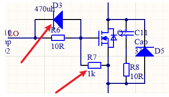
请问为什么8301数据手册的推荐设计,还有8301开发板的设计中下图中的两处设计
1.栅极电阻并联二极管,提供关断电流的低阻泄放路径,缩短关断时间
2.MOS的GS极之间并联电阻,提供GS结电容的泄放路径,防止误导通。
您好,您的问题我们需要升级到英文论坛寻求帮助,如有答复将尽快回复您。
书写错误,改正为:请问为什么8301数据手册的推荐设计,还有8301开发板的设计中没有下图中的两处设计
您好,
虽然在其中有添加/配置了很多有用的电路,但我们很难在数据表中详述每个设计。 如果用户希望实施外部电路来满足其应用、材料、空间和成本需求,我们将会保留各种选项供其选择。 如果存在正常运行所需的任何外部电路,数据表和设计资源中会列出该电路。