Part Number: BQ40Z80
Other Parts Discussed in Thread: BQ40Z50, BQ4050
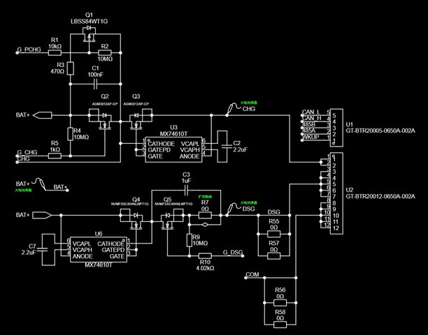
For BQ40Z80, when I wanted to design a parallel charging and discharging circuit (with separate charging and discharging circuits), I chose to connect the PACK pin to the source of the discharge MOS. This would only allow the PACK pin to be used as a reference voltage to control the discharge MOS and lose other functions, resulting in BQ40Z80 being unable to receive voltage from the charger through the PACK pin. However, during use, I did not seem to notice any problems. May I ask if there are any potential risks associated with my design?
By the way, by analogy, do these problems also occur with BQ40Z50 and BQ4050?
对于BQ40Z80,当我希望设计并联的充电放电回路(充电和放电回路分开)时,我选择将PACK引脚连接到放电MOS的源极,那样会使得PACK引脚只能用于作为基准电压控制放电MOS而失去其它功能,从而导致BQ40Z80无法再通过PACK引脚接收来自充电器的电压,但在使用过程中,似乎没有发现问题,请问我这样的设计会有什么潜在风险吗?
顺便问一下,类比地,这些问题是不是也会出现在BQ40Z50、BQ4050身上?
Thank you for your generous response
Martain.