Part Number: BQ25960EVM
Other Parts Discussed in Thread: BQ25960, BQ25980
Hi TI Team!
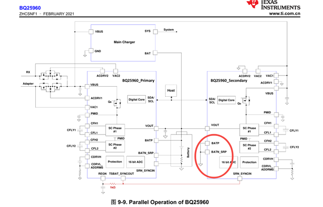
We used two BQ25960 IC,Among them, U1000 was the primary charger, while U1001 was the secondary charger.
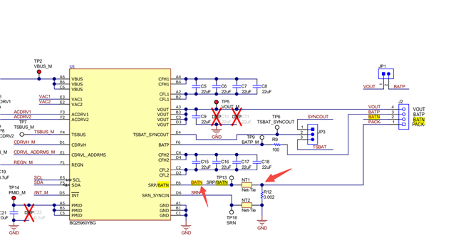
the secondary BQ25960 batp/batn_srp pin connected to the GND in the datasheet but batp/batn_srp pin connected to the battery terminal in the EVM.
1、So, how should this be connected?
2、On primary BQ25960, since there is a certain distance between the current sampling resistor and the negative terminal of the battery, there will be a voltage drop.The SRP/BATN pin simultaneously samples the terminal voltage of the battery negative terminal and the current through the resistance. Whether the detected terminal voltage of the battery negative terminal or the current is inaccurate?
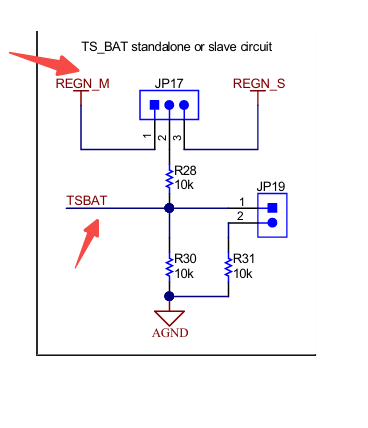
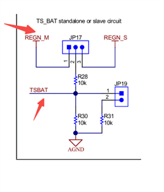
3、Why the secondary BQ25960 TSBAT pull-up power supply set to REGN_M instead of REGN_S?