

Part Number: LM3410-Q1
Other Parts Discussed in Thread: LM3410
Our company is currently utilizing your LM3410 IC in a T-BOX project, where it functions as a charging IC for a backup 0.1C NiMH battery with 600mAh capacity. The input power is a stable 5V output from a primary DC-DC converter.
We are encountering an issue where some ICs are being damaged during the initial charging cycle of the backup battery. For the failed units, we measured approximately 300Ω resistance between VIN pin and GND using a multimeter, while normal chips typically show resistance in the MΩ range. We would appreciate your assistance with the following questions:
-
Could the multimeter measurement method for internal resistance potentially damage the IC?
-
Can the measured internal resistance reliably indicate chip condition or failure severity? (Note: For failed chips, the in-circuit resistance measurements aren't consistent - some show values fluctuating between 900Ω to 2KΩ, yet some still function normally.)
-
Have you encountered similar cases in other projects that might provide reference solutions?
-
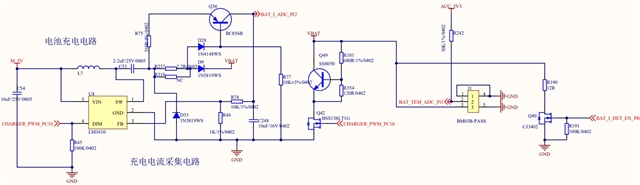
Could you please review our schematic and PCB design to check for any problematic circuits or design flaws that might cause chip damage?
-
If question 2's premise holds true (that resistance indicates chip health), would ICs with lower-than-normal resistance (though currently functioning) be more prone to future failure?
We would greatly appreciate your technical analysis and suggestions regarding these matters.

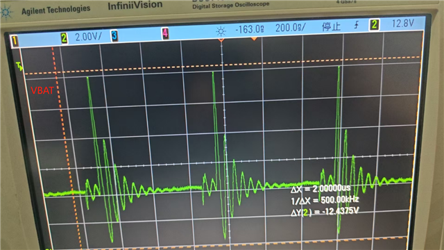
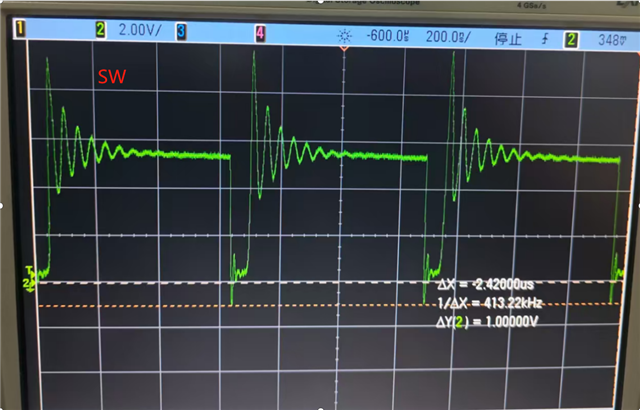

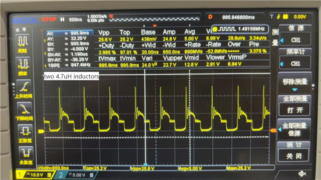 Today, we replaced D33 with a 4.7uH inductor and also changed L7 to 4.7uH. Due to package constraints, we could only use the inductors shown in the figure. The measured waveform is as depicted. After replacing the diode with an inductor, the circuit now operates as a SEPIC topology, which is essentially the same as the circuit in Figure 26 of the datasheet. However, why is the ringing even worse? We’d appreciate your advice on what modifications we should make. (Later, we also tried changing both inductors to 2.2uH, but the ringing waveform remained largely similar.)