If you have a related question, please click the "Ask a related question" button in the top right corner. The newly created question will be automatically linked to this question.
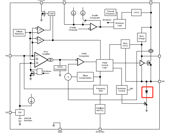
The following operating description of the LMR16030 will refer to the Functional Block Diagram and to the waveforms in Figure 7-1. The LMR16030 output voltage is regulated by turning on the high-side N-MOSFET with controlled ON time. During high-side switch ON time, the SW pin voltage swings up to approximately VIN, and the inductor current iL increases with alinear slope (VIN – VOUT) / L. When the high-side switch is off, inductor current discharges through a freewheel diode with a slope of –VOUT / L. The control parameter of the buck converter is defined as Duty Cycle D = tON / TSW, where tON is the high-side switch ON time and TSW is the switching period. The regulator control loop maintains a constant output voltage by adjusting the duty cycle D. In an ideal buck converter where losses are ignored, D is proportional to the output voltage and inversely proportional to the input voltage: D = VOUT / VIN.