This thread has been locked.

If you have a related question, please click the "Ask a related question" button in the top right corner. The newly created question will be automatically linked to this question.

TIDM-02013: The PFC output voltage drops sharply.

Part Number: TIDM-02013


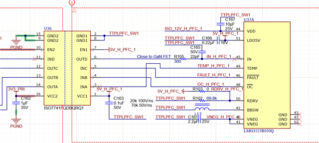
During Lab 1, the PFC (Power Factor Corrector) could normally boost the output voltage when the input DC voltage ranged from 0 to 20V. However, when the input voltage exceeded 20V, after the output voltage surpassed 50V, the output voltage dropped sharply. Within a few seconds, it fell to the same level as the input voltage. I don't understand what the problem is, and my experimental group is currently investigating the issue.

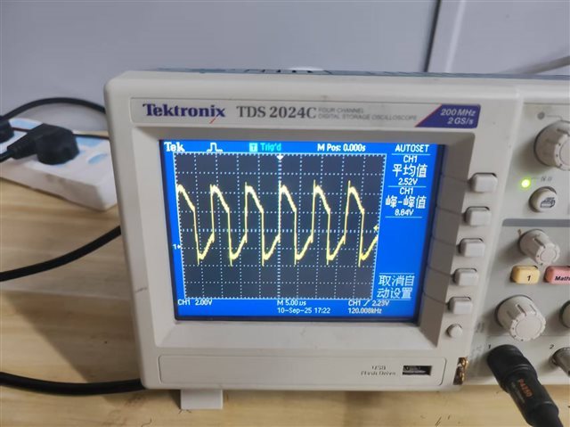
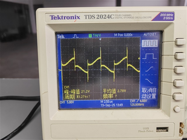
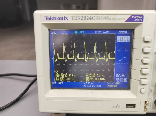
When I adjusted the input voltage from 0V to 10V, I observed that the driving waveform of the upper switch in the GaN PH1 branch was distorted, while the driving waveform of the lower switch remained normal. What could be the cause of this, and would it lead to the aforementioned issue?

  • 您好

    已经收到了您的案例,调查需要些时间,感谢您的耐心等待

  • Hello, the hardware devices I obtained are from the suppliers recommended in the BOM (Bill of Materials). There might be a small number of components that are not entirely identical, but this should not affect the DCLINK.

    The operating steps are as follows:


    1. Connect the auxiliary power supply (11V, 1A).
    2. Run the program in debug mode.
    3. Apply  voltage before the relay closes.
  • Hello, could you please get back to me as soon as possible? My experiment has come to a halt here.

  • 您好

    Did you connect any load on the DC output side of the PFC while conducting above test? May I also know how did you procure this HW board?

  • In the laboratory, I did not connect a load. The components of this device were purchased in accordance with the BOM (Bill of Materials), and there is no essential difference between them.

  • 您好

    May I know if the relay is closed to bypass the PTC resistor?

  • I just tested the relay, and it can effectively bypass the PTC. Could there be any other issues?

  • Hello, I just conducted an experiment. When the input voltage was approximately 30V, the measured voltage at pins 2 and 3 of the diode bridge was 0V, and the output voltage at pins 1 and 4 was also 0V. When my partner and I measured the input voltage of other components, the voltage across capacitor C220 was roughly 30V. After a while, maybe one or two minutes later, the output voltage suddenly rose to the normal level (approximately twice the input voltage). My partner and I gradually increased the input voltage to 110V, at which point the circuit board made a breakdown sound and emitted smoke, and the output voltage dropped sharply afterward. For safety reasons, we terminated the experiment. After remeasuring the circuit board, no issues were found. When we conducted the experiment again, the initial problem occurred. Among all the experiments conducted so far, only the aforementioned one was successful, and moreover, the input voltage did not reach the 120V specified in the experiment manual.

    When no drive signal is applied and the auxiliary power supply is connected to the circuit board, if the MOSFET has no drive, the output voltage equals the input voltage through the diode bridge. However, when the MOSFET on the circuit board is driven, the output voltage drops to 0V, and the voltage across the diode bridge also becomes 0V. What could be the cause of this?

  • 您好

    I can't be sure but it sounds like you destroyed the low frequency FETs in the PFC. These will most likely need to be replaced. I would not recommend powering the board up again until you correct the damage.

    I'm not sure what the issue was with the initial power up. You would need to check for faults to see if the C2K device is turning off the system due to an actual fault condition and then debug that fault. If no fault is present and you are running lab 1 the test results suggest that C2K is turning the system off for some reason or one or more of the FETs are not connected properly.

  • Hello, I am now checking the connection of the MOSFET based on your inference.

  • After testing all MOSFETs to confirm they have drive signals and checking all C2K devices to ensure there are no issues, I started the experiment.

    1: However, when I increased the output voltage, the drive waveform became distorted (as shown in the above oscilloscope diagram). Will the distortion of the drive waveform cause the GaN chip to stop working?

    2: When I connected the oscilloscope across capacitor C165, the output voltage was much lower than the input voltage. When I disconnected the oscilloscope's ground (SW1), the output voltage became equal to the input voltage. I don't understand the reason behind this. Could changes in SW1 cause distortion of the drive signal? Will increasing the capacitance value of C165 improve this situation? Is there a possibility that capacitor C165 is faulty, or could the problem be caused by something else?
  • This is the waveform diagram measuring the voltage between DC_LINK and SW1. According to the SIMULINK simulation, it should present a square wave. This is obviously related to the distortion of the driving waveform. Could this be the key reason for the failure to boost the voltage? (Since the cause of the fault has not been found yet, no high voltage has been input. The input voltage is 10-20V.)

  • Only the upper transistor, with SW1 and SW2 as the ground, has this problem. The driving waveform of the lower transistor and the voltage waveform between SW1 and IPRI SENSE are correct.

  • 您好

    It depends how your test equipment is connected. If the issue only appears when the scope is connected, it could be that your input source is grounded. If it is when you connect the scope ground to the circuit you short out the input diode bridge.

  • But without connecting an oscilloscope, how can I observe the drive waveform?I suspect that the U36 and U40 chips are damaged, and I will try to replace them.

  • In today's experiment, after I replaced U40 and U36, the circuit could normally boost the voltage to around 80V, after which a current breakdown sound occurred. Subsequent measurements showed that when the input voltage was 11V, the output voltage reached 90V. Moreover, the output voltage did not change even after adjusting the duty cycle in CCS, and the following waveform appeared between SW1 and ground. Our team cannot identify the root cause of the problem; we may replace another circuit board later, but we cannot guarantee that the same issue will not occur—and this is exactly what concerns me.

  • 您好

    You will need an oscilloscope. I won't be possible to debug this without one.

  • I have an oscilloscope, but I cannot connect the oscilloscope's ground to SW1 or SW2. After making such a connection, the output voltage drops sharply and the drive waveform becomes distorted. However, when I do not connect the ground to SW1 or SW2, the drive waveform displayed is correct.I will continue debugging this circuit board and hope to make some progress.

  • 您好

    A scope is essential for this task. You should not connect the scope ground to the switch nodes. Also, you can't connect the ground without first understanding how your test equipment is grounded.

  • I have identified the root cause of the problem. The oscilloscope and the auxiliary power supply were connected to the same power strip, which resulted in the ground of the oscilloscope being connected to PGND. This caused SW1 and SW2 to short-circuit with PGND, further leading to a short-circuit between the isolated grounds at both ends of U36 and U40—ultimately triggering the aforementioned issues. I will replace these two chips and conduct the test again. Thank you for your solution.