LMG1210: The Output Waveforms Observed on the HO-HS and LO Ports via Oscilloscope Vary Depending on Whether Both Chips Are Powered Simultaneously

Part Number: LMG1210


Screenshot_2025-10-29-10-08-37-42_99c04817c0de565.jpgScreenshot_2025-10-29-10-08-31-16_99c04817c0de565.jpgScreenshot_2025-10-29-10-10-26-58_99c04817c0de565.jpgScreenshot_2025-10-29-10-10-31-75_99c04817c0de565.jpg

1761704004735.jpg1761703998002.jpg

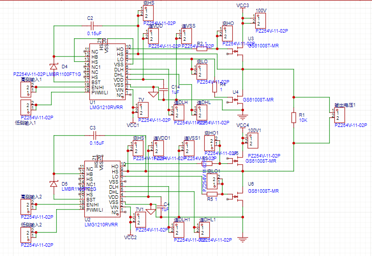
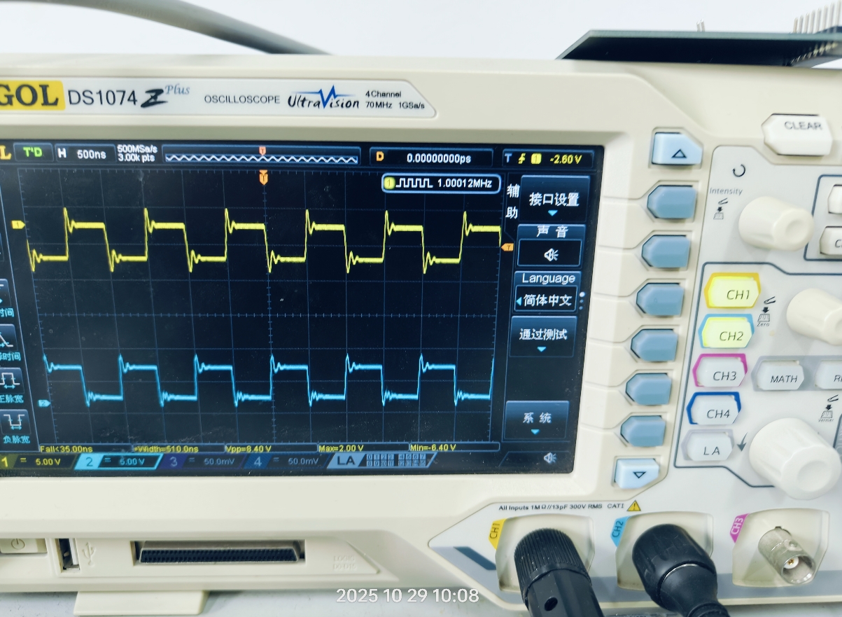
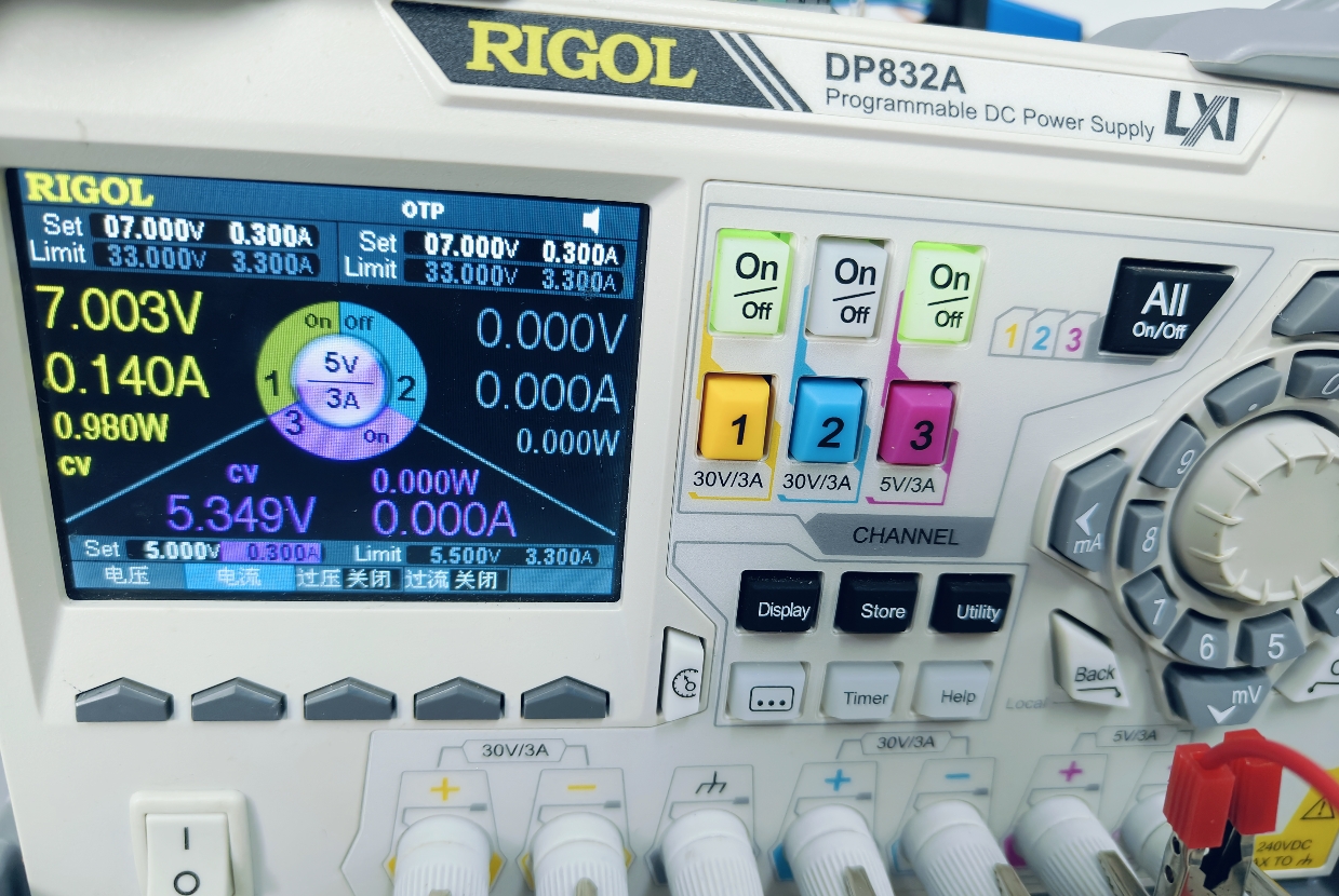
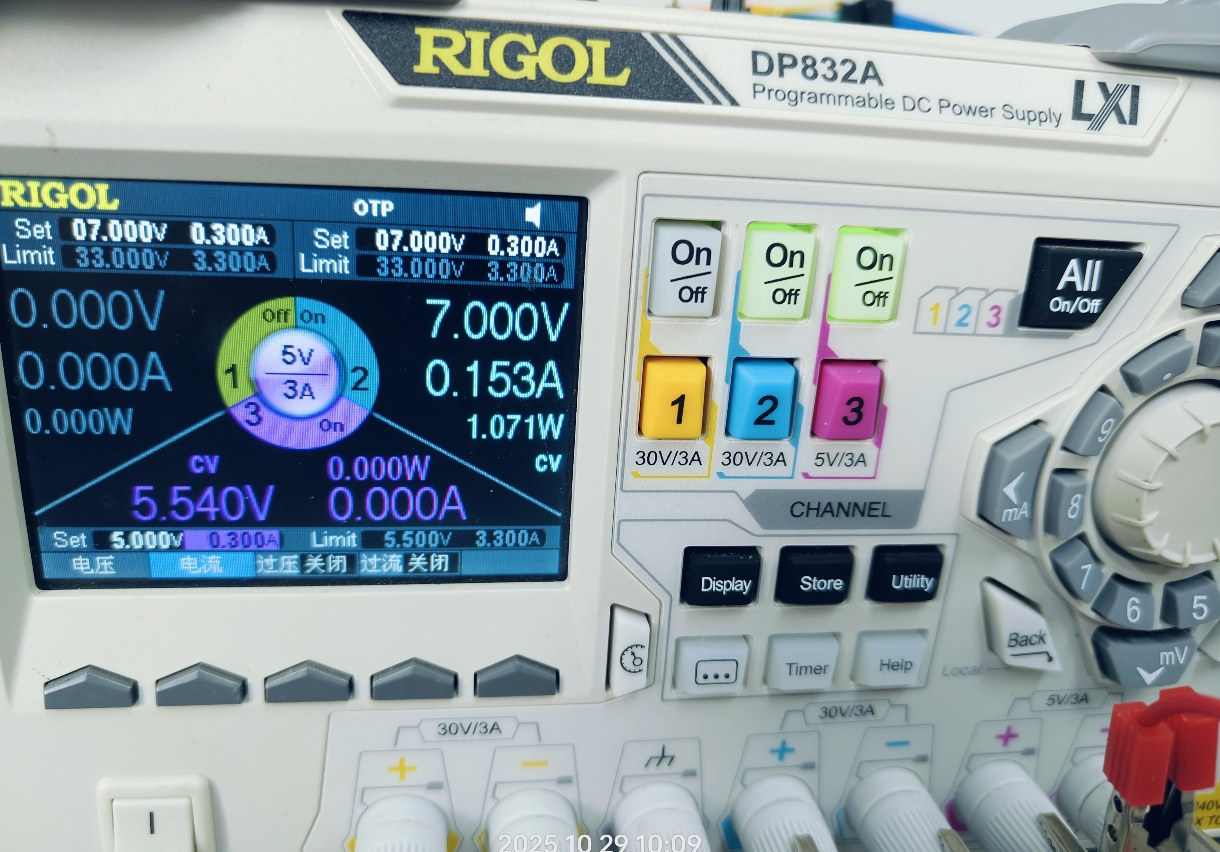
The first image shows the circuit schematic I am using. For this chip, I have chosen the IIM mode. The input signal is a pair of complementary 1MHz PWM signals generated by an FPGA. I encountered an issue: when I power only the first chip (U1) and leave U2 unpowered, the HO-HS and LO ports of the first chip (U1) show normal output, as shown in the second image. The third image shows the power generator settings and the current at that moment.

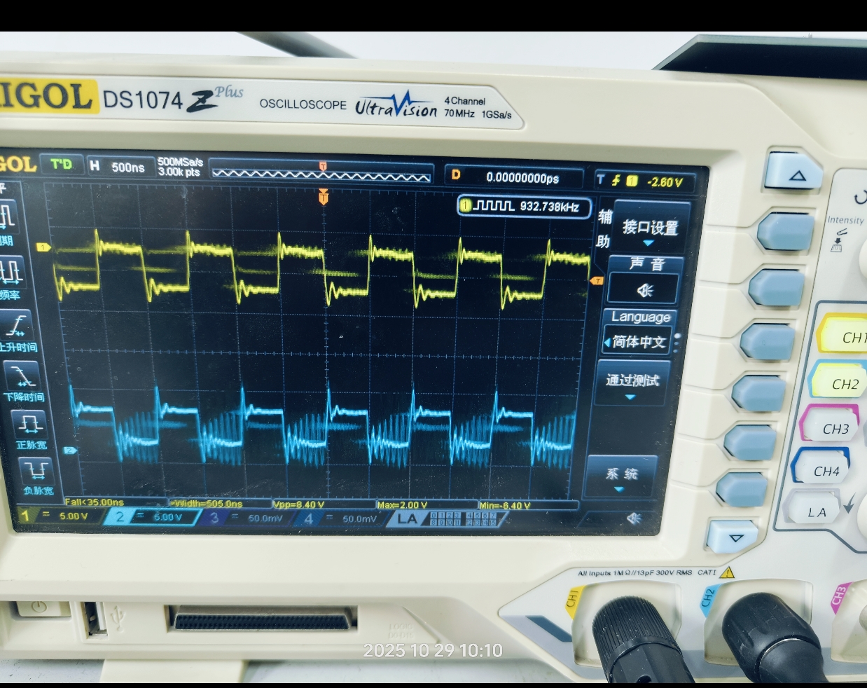
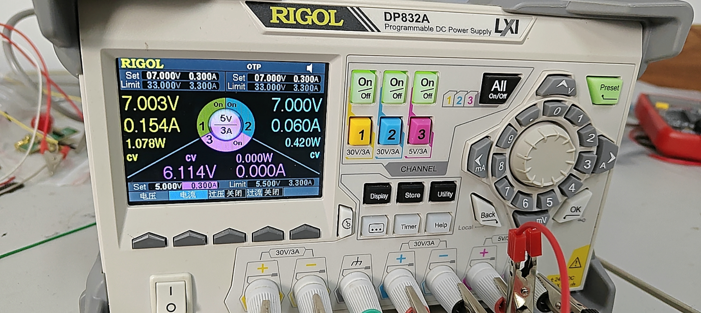
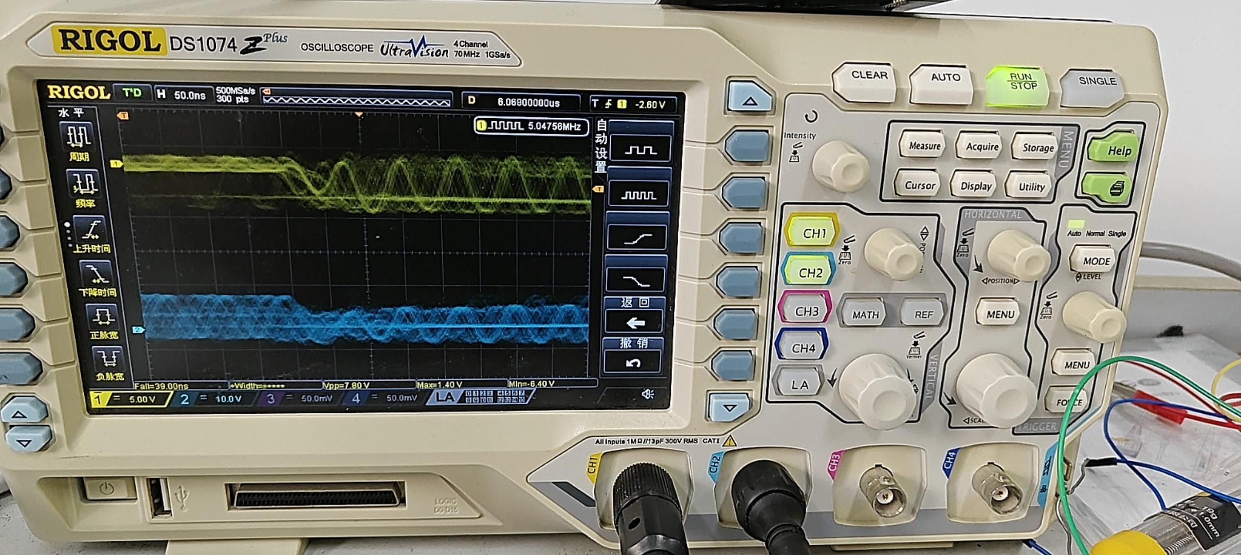
However, when I power only the second chip (U2) and leave U1 unpowered, the HO-HS and LO ports of the second chip (U2) exhibit distortion, as shown in the fourth image. The fifth image shows the power generator settings and current at this point.

When I power both chips simultaneously, no signal is observed, as shown in the seventh image. The settings and current of the power generator at that moment are shown in the sixth image.

At present, I have no clue on how to resolve this issue. Could you provide some troubleshooting suggestions?

  • 已经收到了您的案例,调查需要些时间,感谢您的耐心等待。

  • Thank you for reaching out. In your schematic I see the second driver (U2) does not have the VSS, HS pins/thermal pads connected to each other like you have in first driver (U1). can you clarify if this is done on purpose? 

    Can you make the connections for U2 same as U1 and check if you get the same results or waveforms on U2 as on U1?

  • I sincerely apologize for any misunderstanding caused. On the actual circuit board, the second driver (U2) is interconnected with the VSS, HS pins/thermal pad, just like the first chip.
    Recently, I have identified a new issue. Currently, the chip is in IIM mode. When I apply the same signals to the HI and LI input terminals of the chip, normal PWM waves—with the same frequency and waveform as the input—can be measured at the HO-HS and LO ports without supplying power to VDD. However, when I apply complementary PWM waveforms to the HI and LI input terminals, no output can be detected at the HO-HS and LO ports if VDD is not powered. Why does this difference exist?
    There is another more unusual phenomenon: under the condition of complementary waveform input, if I only supply power to one of the chips while leaving the other unpowered, outputs can still be observed at the HO-HS and LO ports of both chips. Why does this happen?
    I am temporarily unable to figure out how to resolve this problem and would greatly appreciate it if you could provide some troubleshooting suggestions. Thank you very much.